

The foundry also described enhancements to its two chip-stacking techniques, advances in RF CMOS and work in transistors and materials, paving the way to a 3nm node and beyond. In addition, it previewed design capabilities using machine learning that it will offer before the end of the year.
Among its achievements, TSMC noted 76 percent yields on the 256Mbit SRAM made in its first-generation 7nm node, which will be in volume production next year. It also reported that an ARM Cortex-A72 processor in the node exceeded 4GHz using a new design flow.
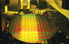
The Taiwan company, already the world’s largest foundry by far, expects to ship 11 million 12-inch-equivalent wafers this year, a typical 10 percent annual increase. The biggest share—two million wafers—will use its planar 28nm processes for which it is boosting capacity 15 percent this year.
TSMC has taped out nearly 800 chips using flavors of its 28nm process. It has shipped 4.5 million 28nm wafers to date, clearly a big sweet spot it aims to defend.
TSMC also plans an ultra-low power version of its 12nm FinFET process, supporting 0.5V operation and starting risk production before June. It will likely be positioned as a competitor to the 12nm FD-SOI process Globalfoundries announced last year but is not expected in production until 2019.
TSMC’s plans to use EUV on an enhanced version of its 7nm process was perhaps the biggest eye opener of the event.
The foundry achieved similar yields using immersion and EUV steppers on a 7nm test chip. In addition, it hit 125W with its ASML 3350 EUV system, providing confidence it can hit about 250W for high volume manufacturing with EUV in 2019 on a 7+nm process.
Samsung announced late last year it plans to use EUV in a 7nm process that could be in production by 2019. “We believe we will be the first one” to use EUV in volume production, said TSMC’s Woo with risk production starting by June 2018.
The company did not detail exactly how it will use EUV steppers except to say it will be at multiple layers. Woo showed a demonstration of EUV 1P1E lines and spaces replacing 4P4E for immersion with “comparable yields and electric performance.”
The 7+ process promises 1.2x greater logic density and 10 percent more speed or 15 percent less power than TSMC’s first-gen 7nm node.
TSMC will start risk production on its first-generation 7nm process next month. It expects in May the first of 12 tapeouts in the process this year, and a total of about 20 tapeouts in the first 12 months.
The process should deliver 3.3x greater routed gate density and either 35 percent more speed or 60 percent less power than the foundry’s 16FF+ node. The process includes new cell libraries, cache macros and serdes.
One TSMC executive said the foundry expects a steep ramp for its 10nm node to 400,000 total wafers this year. He forecast TSMC will make three times as many 10 and 7nm wafers total in 2019. Another executive said volumes of 10nm wafers will surpass 16nm wafers this year.
The 10nm node is expected to be a short lived one, created in large part for Apple’s iPhone 8. It sports twice the gate density, and either 10 percent higher speed or 25 percent less power than the 16nm node, TSMC said.
SOURCE- EETimes

Brian Wang is a Futurist Thought Leader and a popular Science blogger with 1 million readers per month. His blog Nextbigfuture.com is ranked #1 Science News Blog. It covers many disruptive technology and trends including Space, Robotics, Artificial Intelligence, Medicine, Anti-aging Biotechnology, and Nanotechnology.
Known for identifying cutting edge technologies, he is currently a Co-Founder of a startup and fundraiser for high potential early-stage companies. He is the Head of Research for Allocations for deep technology investments and an Angel Investor at Space Angels.
A frequent speaker at corporations, he has been a TEDx speaker, a Singularity University speaker and guest at numerous interviews for radio and podcasts. He is open to public speaking and advising engagements.