
IBM scientists have made carbon nanotube transistors smaller and faster silicon transistors. Carbon nanotube transistors have long had the potential to be better than silicon, but this is the first time when that promise has been realized. Now IBM and others will have to scale up superior carbon nanotube devices.
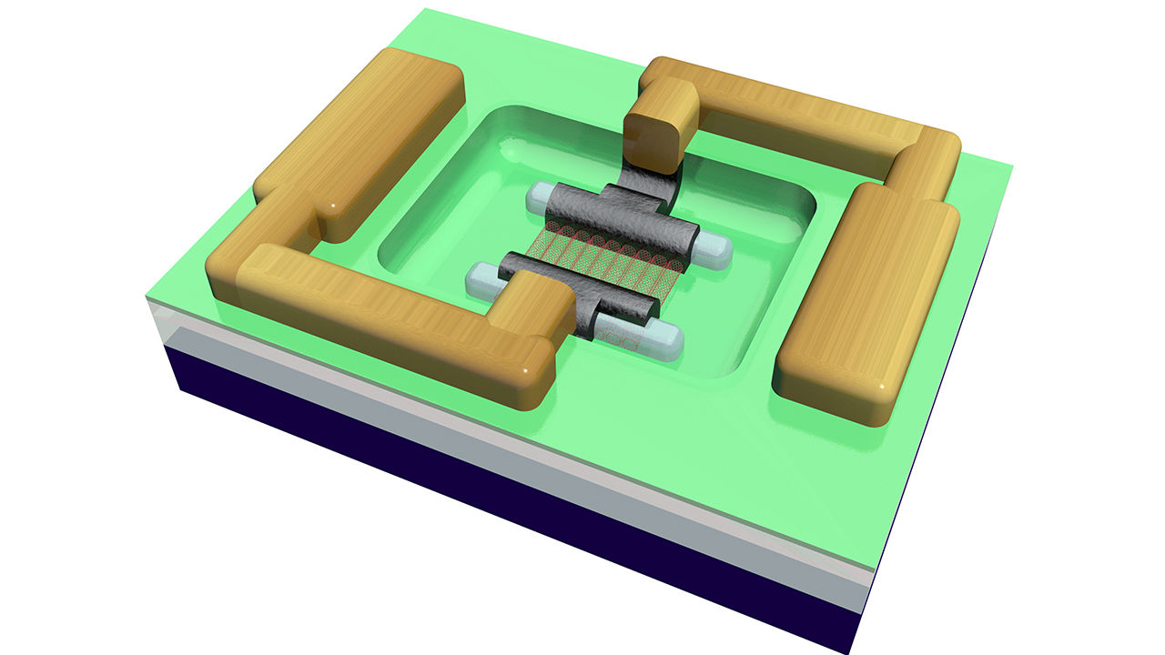
IBM scientists have been experimenting with carbon nanotubes, rolled-up sheets of carbon atoms just 1 nanometer, or a billionth of a meter, in diameter. But difficulties working with the material have meant that, for optimal performance, nanotube transistors have to be even larger than current silicon transistors, which are about 100 nanometers across. To cut that number down, a team of scientists used a new technique to build the contacts that draw current into and out of the carbon nanotube transistor. They constructed the contacts out of molybdenum, which can bond directly to the ends of the nanotubes, making them smaller. They also added cobalt so the bonding could take place at a lower temperature, allowing them to shrink the gap between the contacts. Another advance allowed for practical transistors. Carrying enough electrical current from one contact to another requires several nanotube “wires.” The researchers managed to lay several parallel nanotubes close together in each transistor. The total footprint of the transistor: just 40 nanometers, they report today in Science. Electrical tests showed their new transistors to be faster and more efficient than ones made of silicon.

The International Technology Roadmap for Semiconductors challenged the device research community to reduce the transistor footprint containing all components to 40 nanometers within the next decade. Researchers report on a p-channel transistor scaled to such an extremely small dimension. Built on one semiconducting carbon nanotube, it occupies less than half the space of leading silicon technologies, while delivering a significantly higher pitch-normalized current density—above 0.9 milliampere per micrometer at a low supply voltage of 0.5 volts with a subthreshold swing of 85 millivolts per decade. Furthermore, we show transistors with the same small footprint built on actual high-density arrays of such nanotubes that deliver higher current than that of the best-competing silicon devices under the same overdrive, without any normalization. They achieve this using low-resistance end-bonded contacts, a high-purity semiconducting carbon nanotube source, and self-assembly to pack nanotubes into full surface-coverage aligned arrays.

Brian Wang is a Futurist Thought Leader and a popular Science blogger with 1 million readers per month. His blog Nextbigfuture.com is ranked #1 Science News Blog. It covers many disruptive technology and trends including Space, Robotics, Artificial Intelligence, Medicine, Anti-aging Biotechnology, and Nanotechnology.
Known for identifying cutting edge technologies, he is currently a Co-Founder of a startup and fundraiser for high potential early-stage companies. He is the Head of Research for Allocations for deep technology investments and an Angel Investor at Space Angels.
A frequent speaker at corporations, he has been a TEDx speaker, a Singularity University speaker and guest at numerous interviews for radio and podcasts. He is open to public speaking and advising engagements.