
Scientists at Rutgers University-New Brunswick have learned how to tame the unruly electrons in graphene, paving the way for the ultra-fast transport of electrons with low loss of energy in novel systems.
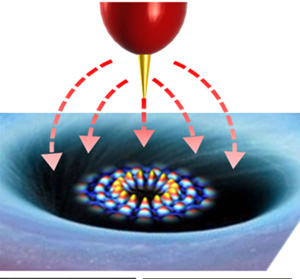
Above – A sharp tip creates a force field that can trap electrons in graphene or modify their trajectories, similar to the effect a lens has on light rays. Yuhang Jiang/Rutgers University-New Brunswick
“This shows we can electrically control the electrons in graphene,” said Eva Y. Andrei, Board of Governors professor in Rutgers’ Department of Physics and Astronomy in the School of Arts and Sciences and the study’s senior author. “In the past, we couldn’t do it. This is the reason people thought that one could not make devices like transistors that require switching with graphene, because their electrons run wild.”
Now it may become possible to realize a graphene nano-scale transistor, Andrei said. Thus far, graphene electronics components include ultrafast amplifiers, supercapacitors and ultralow resistivity wires. The addition of a graphene transistor would be an important step towards an all-graphene electronics platform. Other graphene-based applications include ultrasensitive chemical and biological sensors, filters for desalination and water purification. Graphene is also being developed in flat flexible screens, and paintable and printable electronic circuits.
Graphene is a nano-thin layer of the carbon-based graphite that pencils write with. It is far stronger than steel and a great conductor. But when electrons move through it, they do so in straight lines and their high velocity does not change. “If they hit a barrier, they can’t turn back, so they have to go through it,” Andrei said. “People have been looking at how to control or tame these electrons.”
Her team managed to tame these wild electrons by sending voltage through a high-tech microscope with an extremely sharp tip, also the size of one atom. They created what resembles an optical system by sending voltage through a scanning tunneling microscope, which offers 3-D views of surfaces at the atomic scale. The microscope’s sharp tip creates a force field that traps electrons in graphene or modifies their trajectories, similar to the effect a lens has on light rays. Electrons can easily be trapped and released, providing an efficient on-off switching mechanism, according to Andrei.
“You can trap electrons without making holes in the graphene,” she said. “If you change the voltage, you can release the electrons. So you can catch them and let them go at will.”
The next step would be to scale up by putting extremely thin wires, called nanowires, on top of graphene and controlling the electrons with voltages, she said.
The photon-like propagation of the Dirac electrons in graphene, together with its record-high electronic mobility can lead to applications based on ultrafast electronic response and low dissipation. However, the chiral nature of the charge carriers that is responsible for the high mobility also makes it difficult to control their motion and prevents electronic switching. Here, we show how to manipulate the charge carriers by using a circular p–n junction whose size can be continuously tuned from the nanometre to the micrometre scale. The junction size is controlled with a dual-gate device consisting of a planar back gate and a point-like top gate made by decorating a scanning tunnelling microscope tip with a gold nanowire. The nanometre-scale junction is defined by a deep potential well created by the tip-induced charge. It traps the Dirac electrons in quantum-confined states, which are the graphene equivalent of the atomic collapse states (ACSs) predicted to occur at supercritically charged nuclei. As the junction size increases, the transition to the optical regime is signalled by the emergence of whispering-gallery modes similar to those observed at the perimeter of acoustic or optical resonators, and by the appearance of a Fabry–Pérot interference pattern for junctions close to a boundary.

Brian Wang is a Futurist Thought Leader and a popular Science blogger with 1 million readers per month. His blog Nextbigfuture.com is ranked #1 Science News Blog. It covers many disruptive technology and trends including Space, Robotics, Artificial Intelligence, Medicine, Anti-aging Biotechnology, and Nanotechnology.
Known for identifying cutting edge technologies, he is currently a Co-Founder of a startup and fundraiser for high potential early-stage companies. He is the Head of Research for Allocations for deep technology investments and an Angel Investor at Space Angels.
A frequent speaker at corporations, he has been a TEDx speaker, a Singularity University speaker and guest at numerous interviews for radio and podcasts. He is open to public speaking and advising engagements.
So I have an important question to ask – if electrons are moving masslessly inside the graphene sheet, then does this lower the overall mass of the system as compared to if the electrons were moving inside the graphene in a non-massless way? (ie. when you applied the electric field)
I’m asking in relation to the Mach Effect drive, which is based on mechanically oscillating an object whose mass is changing depending on the direction of oscillation. Graphene can be used as a mechanical oscillator, vibrating like a drumskin. Suppose while the graphene is oscillating in one direction, then you having its electrons moving masslessly, then when the graphene is oscillating in the opposite direction, then you have its electrons move in a non-massless way by applying the electric field. So I’m thinking that would make the graphene heavier when moving one way, and lighter when moving the other way.
Given that graphene can mechanically oscillate at upto gigahertz frequencies, and given that the Mach Effect force is supposed to scale with the cube of frequency, then couldn’t this be the best way to create a stronger and more measurable Mach Effect force? What do you all think?
testing italic font
TEXT HERE
nice
Test result: Failure.
[i]italic[/i]
italic