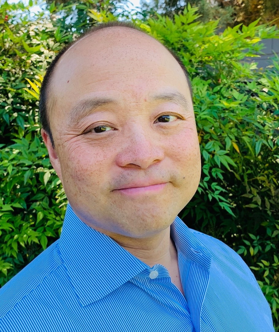
Quantum computer researcher Michelle Simmons was named 2018 Australian of the Year.
A quantum computer is predicted to bring with it an exponential speed up in computational power. This is because instead of performing calculations one after the other like a conventional computer, a quantum computer works in parallel, looking at all the possible outcomes at the same time. The result is massively parallel computing, allowing us to solve problems in minutes that otherwise would take thousands of years.
Michelle Simmons at the University of New South Wales (UNSW) in Sydney, Australia, are developing their own ways of building quantum computers using silicon. In May 2017, she founded an Aus$83 million (US$65 million) start-up called Silicon Quantum Computing, backed in part by the Australian government.
One thinks here of problems where computers work on large data bases or consider lots of variables, problems such as predicting the weather, stock markets, optimising speech, facial and object recognition (such as self-driving cars), looking at optimising aircraft design, targeting drug development to the patients DNA, optimising traffic flow and working out the shortest possible delivery routes. UPS in the US have determined that if they could shorten the distance that every one of their drivers travel each day by one mile, they would save their company $50 million per year. That’s an ideal problem for a quantum computer. But this is a capability with widespread application. Indeed, a US defense firm has predicted that 40 percent of all Australian industry will be impacted if we can realize this technology.
The potential rewards are certainly significant. I firmly believed when I arrived here that we had a viable yet ambitious pathway to get there. Yet when we first proposed our concept, there were many critics all over the world, including senior scientists at IBM who said that whilst it was a nice idea, there were many technical challenges that had to be overcome. We identified eight different steps, none of which had been demonstrated. The consensus view within the global scientific community was that the chances of our getting through all eight stages were near impossible.
On top of this, to make things work, we had to combine two technologies: linking the scanning tunnelling microscope (which provides the ability to measure and manipulate individual atoms) with another technology called molecular beam epitaxy which allows us to grow, layer by layer, material to protect the atoms we have put down.
Both these instruments must operate under ultra-high vacuum, but no one had successfully combined the two, and they seemed incompatible: the STM system needed low vibrational noise to have the sensitivity to image individual atoms, while the MBE system had very large pumps to ensure high purity crystal growth – pumps that caused a great deal of vibration. It was high risk. When I told the two independent system manufacturers in Germany about the idea, they said they would make a system to my design, but that there would be no guarantee that it would work. And for a combined system that cost $3.5 million – that was a pretty big risk!
It took two years from the design of the system to its delivery and set up and was a nail-biting time for my career. It explains where a lot of my grey hairs started to come in). It was hosted in two specially designed adjacent laboratories but connected through the wall.
Did it work? I think I wouldn’t be here if it hadn’t! But to my delight it worked a factor of six better than I had hoped. And over the past decade we have systematically solved all those eight challenges that were predicted to block our way. In fact, the video that you were watching as we came in showed the step by step process we have developed by which we place and build electronic devices using a single phosphorus atom in silicon – the phosphorus being the atom on which we encode information for the atomic-scale computer.
In recent years, we have used this unique technology right here in Sydney to create a stack of world-first atomic-scale devices. We have built the world’s smallest transistor where the active functional part is just a single atom beating those industry predictions from Moore’s Law by nearly a decade. Following this fabricated the world’s narrowest conducting wires in silicon, just four atoms wide with the same current-carrying capability of copper. We are systematically working towards demonstrating all the individual components of a 10 qubit system, which we hope to achieve within the next five years. Using this technique, we have shown that in addition to placing the atoms and wires we have built unique transistors that we can align next to the atoms with sub-nm precision to initialize and read-out information on these atoms. We have demonstrated a concept like entanglement between the atoms where the state of one atom depends on the other – rather like a marriage. It does however had the added ‘quantum’ benefit that both parties can read each other’s mind. It’s a beautiful world to be in.
Finally we have moved to two-, three- and four-qubit architectures and shown our long-term ability using our STM to pattern a 1024 atomic precision array

Brian Wang is a Futurist Thought Leader and a popular Science blogger with 1 million readers per month. His blog Nextbigfuture.com is ranked #1 Science News Blog. It covers many disruptive technology and trends including Space, Robotics, Artificial Intelligence, Medicine, Anti-aging Biotechnology, and Nanotechnology.
Known for identifying cutting edge technologies, he is currently a Co-Founder of a startup and fundraiser for high potential early-stage companies. He is the Head of Research for Allocations for deep technology investments and an Angel Investor at Space Angels.
A frequent speaker at corporations, he has been a TEDx speaker, a Singularity University speaker and guest at numerous interviews for radio and podcasts. He is open to public speaking and advising engagements.

