
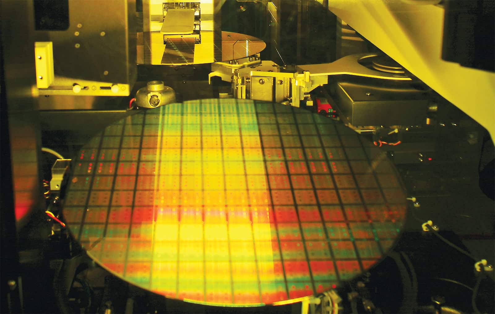
TSMC (Taiwan Semiconductor) taped out its first chip in a process making limited use of extreme ultraviolet lithography and will start risk production in April on a 5-nm node with full EUV.
The foundry’s update showed that area and power gains continue in its leading-edge nodes, but chip speeds are no longer advancing at their historic rate. To compensate, TSMC gave an update on a half-dozen packaging techniques that it is developing to speed connections between chips.
The TSMC N7+ node that can use EUV on up to four layers. Its N5 that will use EUV on up to 14 layers will be ready for risk production in April. EUV aims to lower costs by reducing the number of masks required for leading-edge designs.
Samsung is ramping a 7-nm node using EUV. Intel is not expected to use EUV anytime soon. Globalfoundries announced in August that it has halted work on 7 nm and EUV.
TSMC said that N5 will deliver 14.7% to 17.7% speed gains and 1.8 to 1.86 area shrinks based on tests with Arm A72 cores.

Brian Wang is a Futurist Thought Leader and a popular Science blogger with 1 million readers per month. His blog Nextbigfuture.com is ranked #1 Science News Blog. It covers many disruptive technology and trends including Space, Robotics, Artificial Intelligence, Medicine, Anti-aging Biotechnology, and Nanotechnology.
Known for identifying cutting edge technologies, he is currently a Co-Founder of a startup and fundraiser for high potential early-stage companies. He is the Head of Research for Allocations for deep technology investments and an Angel Investor at Space Angels.
A frequent speaker at corporations, he has been a TEDx speaker, a Singularity University speaker and guest at numerous interviews for radio and podcasts. He is open to public speaking and advising engagements.
You have to think of the 1.8x as a 2D reduction. 7nm x 7nm = an area of 49nm^2. 5nm x 5nm = 25nm^2. That is at least 1.8x smaller (Some connectors can’t be made smaller so they can’t realize the full benefit of 5nm)
You have to think of the 1.8x as a 2D reduction. 7nm x 7nm = an area of 49nm^2. 5nm x 5nm = 25nm^2. That is at least 1.8x smaller (Some connectors can’t be made smaller so they can’t realize the full benefit of 5nm)
You have to think of the 1.8x as a 2D reduction. 7nm x 7nm = an area of 49nm^2. 5nm x 5nm = 25nm^2. That is at least 1.8x smaller (Some connectors can’t be made smaller so they can’t realize the full benefit of 5nm)
You have to think of the 1.8x as a 2D reduction. 7nm x 7nm = an area of 49nm^2. 5nm x 5nm = 25nm^2. That is at least 1.8x smaller (Some connectors can’t be made smaller so they can’t realize the full benefit of 5nm)
You have to think of the 1.8x as a 2D reduction. 7nm x 7nm = an area of 49nm^2. 5nm x 5nm = 25nm^2. That is at least 1.8x smaller (Some connectors can’t be made smaller so they can’t realize the full benefit of 5nm)
If it is just 20% smaller then it is not a amove from 7nm to 5nm 7nm to 5nm would imply a 50% reduction of area
If it is just 20{22800fc54956079738b58e74e4dcd846757aa319aad70fcf90c97a58f3119a12} smaller then it is not a amove from 7nm to 5nm 7nm to 5nm would imply a 50{22800fc54956079738b58e74e4dcd846757aa319aad70fcf90c97a58f3119a12} reduction of area
PS; my list of diacritical modified characters and special UTF–8 symbols is presently 653 &named items. The program itself is 3,300 lines of PERL. Entering in that tert butanoic acid pentahydrate was done type TYPING: (CH3)2COOH⋅(H2O)5. The “chemistry recognizer” detected what looked like well-formed chemical formula, and then turned it into (CH₃)₂COOH⋅(H₂O)₅ all by itself. I didn’t type in a single subscript or have to find that darn small dot. Software — even homebrew — can be remarkably productive when it works right. (Even the long-dashes here were parsed by the script and converted to the right UTF-8 character. And the siggy at the end? I just typed in ‘jsgg’ instead of the whole thing.) Just saying, GoatGuy
PS; my list of diacritical modified characters and special UTF–8 symbols is presently 653 &named items. The program itself is 3300 lines of PERL. Entering in that tert butanoic acid pentahydrate was done type TYPING: (CH3)2COOH⋅(H2O)5. The chemistry recognizer”” detected what looked like well-formed chemical formula”” and then turned it into (CH₃)₂COOH⋅(H₂O)₅ all by itself. I didn’t type in a single subscript or have to find that darn small dot. Software — even homebrew — can be remarkably productive when it works right. (Even the long-dashes here were parsed by the script and converted to the right UTF-8 character. And the siggy at the end? I just typed in ‘jsgg’ instead of the whole thing.)Just saying””GoatGuy”””””””
I’ve just removed ‘commingled’ from my dictionary of words-to-be-lexigraphically-obfuscated-to-get-past-the-censors. (All my comments are post-processed after typing in by a longish program I wrote to do all sorts of useful stuff, like chemistry (CH₂)₃COOH⋅(H₂O)₅ (tert butanoic acid pentahydrate), like math 2⁴ = 16 (exponents) and X₃ (subscripts); it used to allow trivial italicizing, bolding, underlining and a host of other semi-html-ish features common to quite a few weblog comment engines. But now NBF is on VUUKLE, and it has no such features. However, the use of actual subscript and superscript characters (instead of sub and sup tags) has been retained. My program also has a rich set of (&earth ♁), (&moon ☽), (&jupiter ♃) and (&rarr →), (&larr ←) type expanders. Turning them into UTF–8, without having to remember UTF–8. Its been enhanced with non-standard UTF–8 extensions such as (&schwa ə) (&whitecircle ○) and so on. Fun stuff. I really wasn’t pitching the idea of ANOTHER internal coprocessor — with the integrated graphic processor IGP being really as you describe it, essentially an el-cheapo failure. I’m thinking more about a separate coprocessor, like todays very mature GPU chips, which are almost heavenly-sent specialized hyper-processors. But which are also painfully inadequate as AI processors. A processing platform of a new breed. Suitable for inferences, and quantitative but fuzzy concept matching. Thanks for the input. GoatGuy
I’ve just removed ‘commingled’ from my dictionary of words-to-be-lexigraphically-obfuscated-to-get-past-the-censors. (All my comments are post-processed after typing in by a longish program I wrote to do all sorts of useful stuff like chemistry (CH₂)₃COOH⋅(H₂O)₅ (tert butanoic acid pentahydrate) like math 2⁴ = 16 (exponents) and X₃ (subscripts); it used to allow trivial italicizing bolding underlining and a host of other semi-html-ish features common to quite a few weblog comment engines. But now NBF is on VUUKLE and it has no such features. However the use of actual subscript and superscript characters (instead of sub and sup tags) has been retained. My program also has a rich set of (&earth ♁) (&moon ☽) (&jupiter ♃) and (&rarr →) (&larr ←) type expanders. Turning them into UTF–8 without having to remember UTF–8. Its been enhanced with non-standard UTF–8 extensions such as (&schwa ə) (&whitecircle ○) and so on. Fun stuff. I really wasn’t pitching the idea of ANOTHER internal coprocessor — with the integrated graphic processor IGP being really as you describe it essentially an el-cheapo failure. I’m thinking more about a separate coprocessor like todays very mature GPU chips which are almost heavenly-sent specialized hyper-processors. But which are also painfully inadequate as AI processors. A processing platform of a new breed. Suitable for inferences and quantitative but fuzzy concept matching. Thanks for the input.GoatGuy”
I think you misunderstand TSMC technology and what is actually happening. TSMC invests in R&D and produces more wafers than anyone else. TSMC developed 5nm EUV in parralel of 7nm litography and for a long time coming. Further more can we please stop the comparison with intel process now? the one where intel has real process nm node and the others dont? it doesnt even matter since intel doesnt even produce chips for companies they only produce their own designs and thats it so it doesnt matter what process they have. Further more the only comparison that matter is TSMC 7nm+ vs TSMC 5nm EUV, because its their own better production node and companies that will send orders for 5nm EUV will have to compared cost/benefits with TSMC’s 7nm+, or Samsungs. If 5nm EUV is better cost/performance than 7nm+ in any way then it is what it is and its welcome to the market in my book, as long as we ca still have advancements in the process node its still good. Also very important you seem to miss here, 7nm to 5nm in numbers alone is an estimated 40% smaller, if the node is real. Dont get fooled by the small number difference of 2nm, that 2nm is means 40% smaller. Its like moving from 28nm to 20nm or 20nm to 14nm, which is massive leap as we have seen in the past. Ofcourse, yields, clocks, performance, density will all matter, but if TSMC says they can get up to 17% better performance and 1.8 shrinks, which i assume it means actually 20% smaller not 80% or 1.8x, judging by these numbers it means the 5nm EUV process is not optimized to its full potential, instead they went with a safe approach and a small increment from 7nm+ to 5nmEUV, and in the future 5nm+EUV and further will reach that 40% die shrinks, but the first 5nmEUV will probably be a small increment of 20%, still very significant advance for first EUV to market. I assume we will have full 5nm+ EUV with full gains of ~40% smaller node by 2022/2023. 100% they will manage to reach 3nm/3nm+ with EUV for futher gains by 2025
I think you misunderstand TSMC technology and what is actually happening.TSMC invests in R&D and produces more wafers than anyone else.TSMC developed 5nm EUV in parralel of 7nm litography and for a long time coming.Further more can we please stop the comparison with intel process now? the one where intel has real process nm node and the others dont? it doesnt even matter since intel doesnt even produce chips for companies they only produce their own designs and thats it so it doesnt matter what process they have.Further more the only comparison that matter is TSMC 7nm+ vs TSMC 5nm EUV because its their own better production node and companies that will send orders for 5nm EUV will have to compared cost/benefits with TSMC’s 7nm+ or Samsungs.If 5nm EUV is better cost/performance than 7nm+ in any way then it is what it is and its welcome to the market in my book as long as we ca still have advancements in the process node its still good.Also very important you seem to miss here 7nm to 5nm in numbers alone is an estimated 40{22800fc54956079738b58e74e4dcd846757aa319aad70fcf90c97a58f3119a12} smaller if the node is real. Dont get fooled by the small number difference of 2nm that 2nm is means 40{22800fc54956079738b58e74e4dcd846757aa319aad70fcf90c97a58f3119a12} smaller. Its like moving from 28nm to 20nm or 20nm to 14nm which is massive leap as we have seen in the past.Ofcourse yields clocks performance density will all matter but if TSMC says they can get up to 17{22800fc54956079738b58e74e4dcd846757aa319aad70fcf90c97a58f3119a12} better performance and 1.8 shrinks which i assume it means actually 20{22800fc54956079738b58e74e4dcd846757aa319aad70fcf90c97a58f3119a12} smaller not 80{22800fc54956079738b58e74e4dcd846757aa319aad70fcf90c97a58f3119a12} or 1.8x judging by these numbers it means the 5nm EUV process is not optimized to its full potential instead they went with a safe approach and a small increment from 7nm+ to 5nmEUV and in the future 5nm+EUV and fu
now with the same sometimes being cömingled with CPU cores on the same silicon, and now no longer even necessarily driving video animation loads, but actual coprocessors for general purpose computing, just as with that revolution now quite mature, I see a probably inevitable introduction of a new kind of processor specifically for AI. An inference engine. AIE, like GPU. ” I’m not near as optimistic about this. The way I see it the IGP and hybrid computing concept is a failure. Especially hybrid computing, so much so that because of lack of advertising people are not even sure HSA even works on new Ryzen APUs. Not that it matters because no-one at all uses it. But even as an IGP it’s quite a failure. All you get is a compromised CPU combined with a compromised GPU. When I was looking for CPUs saw on cpubench that the ones with IGPs are much weaker for the same price. IGPs are even worse because of the lack of GDDR5 RAM chips. I think we’re far from squeezing in yet another co-processor. PS: Why do you have random diacritics on random words nowadays? (eg: cömingled)
ow with the same sometimes being cömingled with CPU cores on the same silicon and now no longer even necessarily driving video animation loads but actual coprocessors for general purpose computing just as with that revolution now quite mature I see a probably inevitable introduction of a new kind of processor specifically for AI. An inference engine. AIE” like GPU. “”I’m not near as optimistic about this. The way I see it the IGP and hybrid computing concept is a failure. Especially hybrid computing”””” so much so that because of lack of advertising people are not even sure HSA even works on new Ryzen APUs. Not that it matters because no-one at all uses it.But even as an IGP it’s quite a failure. All you get is a compromised CPU combined with a compromised GPU. When I was looking for CPUs saw on cpubench that the ones with IGPs are much weaker for the same price. IGPs are even worse because of the lack of GDDR5 RAM chips.I think we’re far from squeezing in yet another co-processor.PS:Why do you have random diacritics on random words nowadays? (eg: cömingled)”””””””
If it is just 20% smaller then it is not a amove from 7nm to 5nm
7nm to 5nm would imply a 50% reduction of area
PS; my list of diacritical modified characters and special UTF–8 symbols is presently 653 &named items. The program itself is 3,300 lines of PERL. Entering in that tert butanoic acid pentahydrate was done type TYPING: (CH3)2COOH⋅(H2O)5. The “chemistry recognizer” detected what looked like well-formed chemical formula, and then turned it into (CH₃)₂COOH⋅(H₂O)₅ all by itself. I didn’t type in a single subscript or have to find that darn small dot.
Software — even homebrew — can be remarkably productive when it works right. (Even the long-dashes here were parsed by the script and converted to the right UTF-8 character. And the siggy at the end? I just typed in ‘jsgg’ instead of the whole thing.)
Just saying,
GoatGuy
I’ve just removed ‘commingled’ from my dictionary of words-to-be-lexigraphically-obfuscated-to-get-past-the-censors. (All my comments are post-processed after typing in by a longish program I wrote to do all sorts of useful stuff, like chemistry (CH₂)₃COOH⋅(H₂O)₅ (tert butanoic acid pentahydrate), like math 2⁴ = 16 (exponents) and X₃ (subscripts); it used to allow trivial italicizing, bolding, underlining and a host of other semi-html-ish features common to quite a few weblog comment engines.
But now NBF is on VUUKLE, and it has no such features. However, the use of actual subscript and superscript characters (instead of sub and sup tags) has been retained. My program also has a rich set of (&earth ♁), (&moon ☽), (&jupiter ♃) and (&rarr →), (&larr ←) type expanders. Turning them into UTF–8, without having to remember UTF–8. Its been enhanced with non-standard UTF–8 extensions such as (&schwa ə) (&whitecircle ○) and so on. Fun stuff.
I really wasn’t pitching the idea of ANOTHER internal coprocessor — with the integrated graphic processor IGP being really as you describe it, essentially an el-cheapo failure. I’m thinking more about a separate coprocessor, like todays very mature GPU chips, which are almost heavenly-sent specialized hyper-processors. But which are also painfully inadequate as AI processors. A processing platform of a new breed. Suitable for inferences, and quantitative but fuzzy concept matching.
Thanks for the input.
GoatGuy
I think you misunderstand TSMC technology and what is actually happening.
TSMC invests in R&D and produces more wafers than anyone else.
TSMC developed 5nm EUV in parralel of 7nm litography and for a long time coming.
Further more can we please stop the comparison with intel process now? the one where intel has real process nm node and the others dont? it doesnt even matter since intel doesnt even produce chips for companies they only produce their own designs and thats it so it doesnt matter what process they have.
Further more the only comparison that matter is TSMC 7nm+ vs TSMC 5nm EUV, because its their own better production node and companies that will send orders for 5nm EUV will have to compared cost/benefits with TSMC’s 7nm+, or Samsungs.
If 5nm EUV is better cost/performance than 7nm+ in any way then it is what it is and its welcome to the market in my book, as long as we ca still have advancements in the process node its still good.
Also very important you seem to miss here, 7nm to 5nm in numbers alone is an estimated 40% smaller, if the node is real. Dont get fooled by the small number difference of 2nm, that 2nm is means 40% smaller. Its like moving from 28nm to 20nm or 20nm to 14nm, which is massive leap as we have seen in the past.
Ofcourse, yields, clocks, performance, density will all matter, but if TSMC says they can get up to 17% better performance and 1.8 shrinks, which i assume it means actually 20% smaller not 80% or 1.8x, judging by these numbers it means the 5nm EUV process is not optimized to its full potential, instead they went with a safe approach and a small increment from 7nm+ to 5nmEUV, and in the future 5nm+EUV and further will reach that 40% die shrinks, but the first 5nmEUV will probably be a small increment of 20%, still very significant advance for first EUV to market.
I assume we will have full 5nm+ EUV with full gains of ~40% smaller node by 2022/2023.
100% they will manage to reach 3nm/3nm+ with EUV for futher gains by 2025, after that is anyone’s guess.
“now with the same sometimes being cömingled with CPU cores on the same silicon, and now no longer even necessarily driving video animation loads, but actual coprocessors for general purpose computing, just as with that revolution now quite mature, I see a probably inevitable introduction of a new kind of processor specifically for AI. An inference engine. AIE, like GPU. ”
I’m not near as optimistic about this. The way I see it the IGP and hybrid computing concept is a failure. Especially hybrid computing, so much so that because of lack of advertising people are not even sure HSA even works on new Ryzen APUs. Not that it matters because no-one at all uses it.
But even as an IGP it’s quite a failure. All you get is a compromised CPU combined with a compromised GPU. When I was looking for CPUs saw on cpubench that the ones with IGPs are much weaker for the same price. IGPs are even worse because of the lack of GDDR5 RAM chips.
I think we’re far from squeezing in yet another co-processor.
PS:
Why do you have random diacritics on random words nowadays? (eg: cömingled)
Sorry but I do not buy it.. Look, I still remember when Intel was promising a 5Ghz chip in the early 2000s or was it in the late 1990s? And then a 10GHz chip soon later. We are still stuck with 4GHZ chips almost two decades later. Sure EUV enables to litho 5nm chips (which means 7nm chips Intel way) but other issues are around the corner, pellicles , quantum tunneling and so on.. It took Intel, the ex-best semi company in town , 5 years to go to 14nm (10nm TSMC way) to 10nm (7nm in TSMCway) and now the Taiwanese claim to go from 7 to 5 in just two years? What are they? Magicians? Unless they are rebranding a 7nm+ as a 5nm .. Let alone I am not sure what 1.8 area shrinks means. Does it mean the total area shrnikns by 80%? or what? Or by 1.8 times? Not very clear.. Still I doubt this will happen If they wham! do it, then Intel will go bankrupt as they are still stuck with 14nm as for now (two generations, not three, behind the taiwanese 5nm process) So even if Intel pulls out the 10nm feat, they will still be behind one generation the Taiwanese 5nm.. Ver unlikely..
Sorry but I do not buy it.. Look I still remember when Intel was promising a 5Ghz chip in the early 2000s or was it in the late 1990s? And then a 10GHz chip soon later. We are still stuck with 4GHZ chips almost two decades later. Sure EUV enables to litho 5nm chips (which means 7nm chips Intel way) but other issues are around the corner pellicles quantum tunneling and so on.. It took Intel the ex-best semi company in town 5 years to go to 14nm (10nm TSMC way) to 10nm (7nm in TSMCway) and now the Taiwanese claim to go from 7 to 5 in just two years? What are they? Magicians? Unless they are rebranding a 7nm+ as a 5nm .. Let alone I am not sure what 1.8 area shrinks means. Does it mean the total area shrnikns by 80{22800fc54956079738b58e74e4dcd846757aa319aad70fcf90c97a58f3119a12}? or what? Or by 1.8 times? Not very clear.. Still I doubt this will happen If they wham! do it then Intel will go bankrupt as they are still stuck with 14nm as for now (two generations not three behind the taiwanese 5nm process) So even if Intel pulls out the 10nm feat they will still be behind one generation the Taiwanese 5nm.. Ver unlikely..
I’m betting that this innovation will usher out the “next revolution” in chipmaking. Its about time: EUV was being seriously researched as long ago as 2000. There was a LOT of prototype machines made after 2010. Now we’re coming on the close of 2018. Thing is, once this takes hold for the premium-priced high-end market, it will rapidly be wanted for the lower end stuff. 5 nm chips, with 10 to 15 nm traces (“wiring”) can really significantly squeeze something like a single core of a Ryzen (AMD competition to Intel’s i5 i7 i9 chips) to darn small proportions. So squeezed, the obvious game is “just lay down more of them, to compete”. Oh, it is a bit of a hollow stance if the effect of supporting cache memory isn’t enough to keep all the tiny cores fully loaded, but when chip speeds will jump likely to 6 GHz and beyond just due to the shrinking dimension, its kind of hard to say what the revolution will ultimately hatch. AI is showing signs of making it past its putative infancy and into more mature “adulthood”. And a lot of work has gone into figuring out what kind of computing facilities are needed “at the core” to get AI done with sufficient sophistication and speed to feel like “real time” to users using it. Just in the say a at-first-quiet-then-much-soapboxed revolution in coprocessors came about starting in the 1990s with GPUS on video cards, and so on, now with the same sometimes being cömingled with CPU cores on the same silicon, and now no longer even necessarily driving video animation loads, but actual coprocessors for general purpose computing, just as with that revolution now quite mature, I see a probably inevitable introduction of a new kind of processor specifically for AI. An inference engine. AIE, like GPU. One thing would be for certain: such an AIE would definitely require a quadruple boatload of not-hard-wired processing. And wicked memory bandwidth. Trillions of inferences per second, substantial inference depth, retention of
I’m betting that this innovation will usher out the “next revolution” in chipmaking. Its about time: EUV was being seriously researched as long ago as 2000. There was a LOT of prototype machines made after 2010. Now we’re coming on the close of 2018. Thing is once this takes hold for the premium-priced high-end market it will rapidly be wanted for the lower end stuff. 5 nm chips with 10 to 15 nm traces (wiring””) can really significantly squeeze something like a single core of a Ryzen (AMD competition to Intel’s i5 i7 i9 chips) to darn small proportions. So squeezed”” the obvious game is “just lay down more of them to compete”. Oh it is a bit of a hollow stance if the effect of supporting cache memory isn’t enough to keep all the tiny cores fully loaded but when chip speeds will jump likely to 6 GHz and beyond just due to the shrinking dimension”” its kind of hard to say what the revolution will ultimately hatch. AI is showing signs of making it past its putative infancy and into more mature “adulthood”. And a lot of work has gone into figuring out what kind of computing facilities are needed “at the core” to get AI done with sufficient sophistication and speed to feel like “”””real time”””” to users using it. Just in the say a at-first-quiet-then-much-soapboxed revolution in coprocessors came about starting in the 1990s with GPUS on video cards”” and so on now with the same sometimes being cömingled with CPU cores on the same silicon and now no longer even necessarily driving video animation loads but actual coprocessors for general purpose computing just as with that revolution now quite mature I see a probably inevitable introduction of a new kind of processor specifically for AI. An inference engine. AIE like GPU.One thing would be for certain: such an AIE would definitely require a quadruple boatload of not-hard-wired processing. And wicked memory bandwidth. Trillions of inferences per second substantial inference depth reten”
YES… technically it can get smaller. Down to about 2 nanometers or thereabouts. Turns out that much below that and quantum effects become excessive. Actually more like “statistical effects”. Remembering that the basic unit of digital computing is the FET gate (these days), and remembering in turn that an FET consists of 3 primary features: a channel, the end-connections and an insulated gate straddling the channel, it then is instructive to consider the channel. Its length — like that of a rope — determines in large part how quickly electrons entering one end make it to the other end. Unlike the fourth part of every semiconductor gate, the “stuff around it, in which it was implanted” (AKA “substrate”), the channel has had a very tiny buttload of ions implanted in it which enhance its conduction either of electrons or holes¹. But the point is, its conduction properties are significantly altered by the ions implanted in it. Now it turns out that the indiviual atoms in the crystal lattice might be as little as 2.35Â âhngstroms (0.235 nm) from each other. When the channel is around 5 nm wide and only 2 nm long, there are what, 10 nm² or 1,000Â of unit area? And the thing might be 10 atoms thick. volume = (20Â ÷ 2.35) • (50Â ÷ 2.35) × 10 = 1,800 atoms The doping (implanted ions) might be a few percent. Well… that’s only 36 atoms at 2%. Needless to say, across a whole wafer of trillions or quadrillions of gates, there’s going to be quite a bit of “at the rails” gaussian variation of the channel implanting ratios. Thus, statistically many transistors may be duds. Just saying, GoatGuy ________________________________________ ¹ holes – kind of ‘anti electrons’ or carriers of + charge, not – charge. They are vacancies in the otherwise covalently filled crystal lattice of the silicon (or whatever the chosen semiconductor is).
YES… technically it can get smaller. Down to about 2 nanometers or thereabouts. Turns out that much below that and quantum effects become excessive. Actually more like “statistical effects”. Remembering that the basic unit of digital computing is the FET gate (these days) and remembering in turn that an FET consists of 3 primary features: a channel the end-connections and an insulated gate straddling the channel it then is instructive to consider the channel. Its length — like that of a rope — determines in large part how quickly electrons entering one end make it to the other end. Unlike the fourth part of every semiconductor gate the “stuff around it in which it was implanted” (AKA substrate””)”” the channel has had a very tiny buttload of ions implanted in it which enhance its conduction either of electrons or holes¹. But the point is its conduction properties are significantly altered by the ions implanted in it. Now it turns out that the indiviual atoms in the crystal lattice might be as little as 2.35Â âhngstroms (0.235 nm) from each other. When the channel is around 5 nm wide and only 2 nm long there are what 10 nm² or 1000Â of unit area? And the thing might be 10 atoms thick. volume = (20Â ÷ 2.35) • (50Â ÷ 2.35) × 10 = 1800 atomsThe doping (implanted ions) might be a few percent. Well… that’s only 36 atoms at 2{22800fc54956079738b58e74e4dcd846757aa319aad70fcf90c97a58f3119a12}. Needless to say across a whole wafer of trillions or quadrillions of gates”” there’s going to be quite a bit of “”””at the rails”””” gaussian variation of the channel implanting ratios. Thus”” statistically many transistors may be duds. Just sayingGoatGuy________________________________________¹ holes – kind of ‘anti electrons’ or carriers of + charge”” not – charge. They are vacancies in the otherwise covalently filled crystal lattice of the silicon (or whatever the chosen semiconductor is).”””””””
So that’s it right? Can’t get smaller, right?
So that’s it right? Can’t get smaller right?
Sorry but I do not buy it..
Look, I still remember when Intel was promising a 5Ghz chip in the early 2000s or was it in the late 1990s?
And then a 10GHz chip soon later.
We are still stuck with 4GHZ chips almost two decades later.
Sure EUV enables to litho 5nm chips (which means 7nm chips Intel way) but other issues are around the corner, pellicles , quantum tunneling and so on..
It took Intel, the ex-best semi company in town , 5 years to go to 14nm (10nm TSMC way) to 10nm (7nm in TSMCway) and now the Taiwanese claim to go from 7 to 5 in just two years?
What are they? Magicians?
Unless they are rebranding a 7nm+ as a 5nm ..
Let alone I am not sure what 1.8 area shrinks means.
Does it mean the total area shrnikns by 80%?
or what?
Or by 1.8 times?
Not very clear..
Still I doubt this will happen
If they wham! do it, then Intel will go bankrupt as they are still stuck with 14nm as for now (two generations, not three, behind the taiwanese 5nm process) So even if Intel pulls out the 10nm feat, they will still be behind one generation the Taiwanese 5nm..
Ver unlikely..
I’m betting that this innovation will usher out the “next revolution” in chipmaking. Its about time: EUV was being seriously researched as long ago as 2000. There was a LOT of prototype machines made after 2010. Now we’re coming on the close of 2018.
Thing is, once this takes hold for the premium-priced high-end market, it will rapidly be wanted for the lower end stuff. 5 nm chips, with 10 to 15 nm traces (“wiring”) can really significantly squeeze something like a single core of a Ryzen (AMD competition to Intel’s i5 i7 i9 chips) to darn small proportions.
So squeezed, the obvious game is “just lay down more of them, to compete”. Oh, it is a bit of a hollow stance if the effect of supporting cache memory isn’t enough to keep all the tiny cores fully loaded, but when chip speeds will jump likely to 6 GHz and beyond just due to the shrinking dimension, its kind of hard to say what the revolution will ultimately hatch.
AI is showing signs of making it past its putative infancy and into more mature “adulthood”. And a lot of work has gone into figuring out what kind of computing facilities are needed “at the core” to get AI done with sufficient sophistication and speed to feel like “real time” to users using it.
Just in the say a at-first-quiet-then-much-soapboxed revolution in coprocessors came about starting in the 1990s with GPUS on video cards, and so on, now with the same sometimes being cömingled with CPU cores on the same silicon, and now no longer even necessarily driving video animation loads, but actual coprocessors for general purpose computing, just as with that revolution now quite mature, I see a probably inevitable introduction of a new kind of processor specifically for AI. An inference engine. AIE, like GPU.
One thing would be for certain: such an AIE would definitely require a quadruple boatload of not-hard-wired processing. And wicked memory bandwidth. Trillions of inferences per second, substantial inference depth, retention of precomputed inference trees and so on.
Which EUV is very, very likely to enable.
For — at first — a few thousand watts, then a few hundred, then under a hundred, and under a thousand bucks. 2020, perhaps? I don’t think that’s too soon, nor too far off.
Just saying,
GoatGuy
YES… technically it can get smaller. Down to about 2 nanometers or thereabouts. Turns out that much below that and quantum effects become excessive. Actually more like “statistical effects”. Remembering that the basic unit of digital computing is the FET gate (these days), and remembering in turn that an FET consists of 3 primary features: a channel, the end-connections and an insulated gate straddling the channel, it then is instructive to consider the channel.
Its length — like that of a rope — determines in large part how quickly electrons entering one end make it to the other end. Unlike the fourth part of every semiconductor gate, the “stuff around it, in which it was implanted” (AKA “substrate”), the channel has had a very tiny buttload of ions implanted in it which enhance its conduction either of electrons or holes¹. But the point is, its conduction properties are significantly altered by the ions implanted in it.
Now it turns out that the indiviual atoms in the crystal lattice might be as little as 2.35Â âhngstroms (0.235 nm) from each other. When the channel is around 5 nm wide and only 2 nm long, there are what, 10 nm² or 1,000Â of unit area? And the thing might be 10 atoms thick.
volume = (20Â ÷ 2.35) • (50Â ÷ 2.35) × 10 = 1,800 atoms
The doping (implanted ions) might be a few percent. Well… that’s only 36 atoms at 2%. Needless to say, across a whole wafer of trillions or quadrillions of gates, there’s going to be quite a bit of “at the rails” gaussian variation of the channel implanting ratios. Thus, statistically many transistors may be duds.
Just saying,
GoatGuy
________________________________________
¹ holes – kind of ‘anti electrons’ or carriers of + charge, not – charge. They are vacancies in the otherwise covalently filled crystal lattice of the silicon (or whatever the chosen semiconductor is).
So that’s it right? Can’t get smaller, right?
PS; my list of diacritical modified characters and special UTF–8 symbols is presently 653 &named items. The program itself is 3,300 lines of PERL. Entering in that tert butanoic acid pentahydrate was done type TYPING: (CH3)2COOH⋅(H2O)5. The “chemistry recognizer” detected what looked like well-formed chemical formula, and then turned it into (CH₃)₂COOH⋅(H₂O)₅ all by itself. I didn’t type in a single subscript or have to find that darn small dot. Software — even homebrew — can be remarkably productive when it works right. (Even the long-dashes here were parsed by the script and converted to the right UTF-8 character. And the siggy at the end? I just typed in ‘jsgg’ instead of the whole thing.) Just saying, GoatGuy
PS; my list of diacritical modified characters and special UTF–8 symbols is presently 653 &named items. The program itself is 3300 lines of PERL. Entering in that tert butanoic acid pentahydrate was done type TYPING: (CH3)2COOH⋅(H2O)5. The chemistry recognizer”” detected what looked like well-formed chemical formula”” and then turned it into (CH₃)₂COOH⋅(H₂O)₅ all by itself. I didn’t type in a single subscript or have to find that darn small dot. Software — even homebrew — can be remarkably productive when it works right. (Even the long-dashes here were parsed by the script and converted to the right UTF-8 character. And the siggy at the end? I just typed in ‘jsgg’ instead of the whole thing.)Just saying””GoatGuy”””””””
I’ve just removed ‘commingled’ from my dictionary of words-to-be-lexigraphically-obfuscated-to-get-past-the-censors. (All my comments are post-processed after typing in by a longish program I wrote to do all sorts of useful stuff, like chemistry (CH₂)₃COOH⋅(H₂O)₅ (tert butanoic acid pentahydrate), like math 2⁴ = 16 (exponents) and X₃ (subscripts); it used to allow trivial italicizing, bolding, underlining and a host of other semi-html-ish features common to quite a few weblog comment engines. But now NBF is on VUUKLE, and it has no such features. However, the use of actual subscript and superscript characters (instead of sub and sup tags) has been retained. My program also has a rich set of (&earth ♁), (&moon ☽), (&jupiter ♃) and (&rarr →), (&larr ←) type expanders. Turning them into UTF–8, without having to remember UTF–8. Its been enhanced with non-standard UTF–8 extensions such as (&schwa ə) (&whitecircle ○) and so on. Fun stuff. I really wasn’t pitching the idea of ANOTHER internal coprocessor — with the integrated graphic processor IGP being really as you describe it, essentially an el-cheapo failure. I’m thinking more about a separate coprocessor, like todays very mature GPU chips, which are almost heavenly-sent specialized hyper-processors. But which are also painfully inadequate as AI processors. A processing platform of a new breed. Suitable for inferences, and quantitative but fuzzy concept matching. Thanks for the input. GoatGuy
I’ve just removed ‘commingled’ from my dictionary of words-to-be-lexigraphically-obfuscated-to-get-past-the-censors. (All my comments are post-processed after typing in by a longish program I wrote to do all sorts of useful stuff like chemistry (CH₂)₃COOH⋅(H₂O)₅ (tert butanoic acid pentahydrate) like math 2⁴ = 16 (exponents) and X₃ (subscripts); it used to allow trivial italicizing bolding underlining and a host of other semi-html-ish features common to quite a few weblog comment engines. But now NBF is on VUUKLE and it has no such features. However the use of actual subscript and superscript characters (instead of sub and sup tags) has been retained. My program also has a rich set of (&earth ♁) (&moon ☽) (&jupiter ♃) and (&rarr →) (&larr ←) type expanders. Turning them into UTF–8 without having to remember UTF–8. Its been enhanced with non-standard UTF–8 extensions such as (&schwa ə) (&whitecircle ○) and so on. Fun stuff. I really wasn’t pitching the idea of ANOTHER internal coprocessor — with the integrated graphic processor IGP being really as you describe it essentially an el-cheapo failure. I’m thinking more about a separate coprocessor like todays very mature GPU chips which are almost heavenly-sent specialized hyper-processors. But which are also painfully inadequate as AI processors. A processing platform of a new breed. Suitable for inferences and quantitative but fuzzy concept matching. Thanks for the input.GoatGuy”
I think you misunderstand TSMC technology and what is actually happening. TSMC invests in R&D and produces more wafers than anyone else. TSMC developed 5nm EUV in parralel of 7nm litography and for a long time coming. Further more can we please stop the comparison with intel process now? the one where intel has real process nm node and the others dont? it doesnt even matter since intel doesnt even produce chips for companies they only produce their own designs and thats it so it doesnt matter what process they have. Further more the only comparison that matter is TSMC 7nm+ vs TSMC 5nm EUV, because its their own better production node and companies that will send orders for 5nm EUV will have to compared cost/benefits with TSMC’s 7nm+, or Samsungs. If 5nm EUV is better cost/performance than 7nm+ in any way then it is what it is and its welcome to the market in my book, as long as we ca still have advancements in the process node its still good. Also very important you seem to miss here, 7nm to 5nm in numbers alone is an estimated 40% smaller, if the node is real. Dont get fooled by the small number difference of 2nm, that 2nm is means 40% smaller. Its like moving from 28nm to 20nm or 20nm to 14nm, which is massive leap as we have seen in the past. Ofcourse, yields, clocks, performance, density will all matter, but if TSMC says they can get up to 17% better performance and 1.8 shrinks, which i assume it means actually 20% smaller not 80% or 1.8x, judging by these numbers it means the 5nm EUV process is not optimized to its full potential, instead they went with a safe approach and a small increment from 7nm+ to 5nmEUV, and in the future 5nm+EUV and further will reach that 40% die shrinks, but the first 5nmEUV will probably be a small increment of 20%, still very significant advance for first EUV to market. I assume we will have full 5nm+ EUV with full gains of ~40% smaller node by 2022/2023. 100% they will manage to reach 3nm/3nm+ with EUV for futher gains by 2025
I think you misunderstand TSMC technology and what is actually happening.TSMC invests in R&D and produces more wafers than anyone else.TSMC developed 5nm EUV in parralel of 7nm litography and for a long time coming.Further more can we please stop the comparison with intel process now? the one where intel has real process nm node and the others dont? it doesnt even matter since intel doesnt even produce chips for companies they only produce their own designs and thats it so it doesnt matter what process they have.Further more the only comparison that matter is TSMC 7nm+ vs TSMC 5nm EUV because its their own better production node and companies that will send orders for 5nm EUV will have to compared cost/benefits with TSMC’s 7nm+ or Samsungs.If 5nm EUV is better cost/performance than 7nm+ in any way then it is what it is and its welcome to the market in my book as long as we ca still have advancements in the process node its still good.Also very important you seem to miss here 7nm to 5nm in numbers alone is an estimated 40{22800fc54956079738b58e74e4dcd846757aa319aad70fcf90c97a58f3119a12} smaller if the node is real. Dont get fooled by the small number difference of 2nm that 2nm is means 40{22800fc54956079738b58e74e4dcd846757aa319aad70fcf90c97a58f3119a12} smaller. Its like moving from 28nm to 20nm or 20nm to 14nm which is massive leap as we have seen in the past.Ofcourse yields clocks performance density will all matter but if TSMC says they can get up to 17{22800fc54956079738b58e74e4dcd846757aa319aad70fcf90c97a58f3119a12} better performance and 1.8 shrinks which i assume it means actually 20{22800fc54956079738b58e74e4dcd846757aa319aad70fcf90c97a58f3119a12} smaller not 80{22800fc54956079738b58e74e4dcd846757aa319aad70fcf90c97a58f3119a12} or 1.8x judging by these numbers it means the 5nm EUV process is not optimized to its full potential instead they went with a safe approach and a small increment from 7nm+ to 5nmEUV and in the future 5nm+EUV and fu
now with the same sometimes being cömingled with CPU cores on the same silicon, and now no longer even necessarily driving video animation loads, but actual coprocessors for general purpose computing, just as with that revolution now quite mature, I see a probably inevitable introduction of a new kind of processor specifically for AI. An inference engine. AIE, like GPU. ” I’m not near as optimistic about this. The way I see it the IGP and hybrid computing concept is a failure. Especially hybrid computing, so much so that because of lack of advertising people are not even sure HSA even works on new Ryzen APUs. Not that it matters because no-one at all uses it. But even as an IGP it’s quite a failure. All you get is a compromised CPU combined with a compromised GPU. When I was looking for CPUs saw on cpubench that the ones with IGPs are much weaker for the same price. IGPs are even worse because of the lack of GDDR5 RAM chips. I think we’re far from squeezing in yet another co-processor. PS: Why do you have random diacritics on random words nowadays? (eg: cömingled)
ow with the same sometimes being cömingled with CPU cores on the same silicon and now no longer even necessarily driving video animation loads but actual coprocessors for general purpose computing just as with that revolution now quite mature I see a probably inevitable introduction of a new kind of processor specifically for AI. An inference engine. AIE” like GPU. “”I’m not near as optimistic about this. The way I see it the IGP and hybrid computing concept is a failure. Especially hybrid computing”””” so much so that because of lack of advertising people are not even sure HSA even works on new Ryzen APUs. Not that it matters because no-one at all uses it.But even as an IGP it’s quite a failure. All you get is a compromised CPU combined with a compromised GPU. When I was looking for CPUs saw on cpubench that the ones with IGPs are much weaker for the same price. IGPs are even worse because of the lack of GDDR5 RAM chips.I think we’re far from squeezing in yet another co-processor.PS:Why do you have random diacritics on random words nowadays? (eg: cömingled)”””””””
Sorry but I do not buy it.. Look, I still remember when Intel was promising a 5Ghz chip in the early 2000s or was it in the late 1990s? And then a 10GHz chip soon later. We are still stuck with 4GHZ chips almost two decades later. Sure EUV enables to litho 5nm chips (which means 7nm chips Intel way) but other issues are around the corner, pellicles , quantum tunneling and so on.. It took Intel, the ex-best semi company in town , 5 years to go to 14nm (10nm TSMC way) to 10nm (7nm in TSMCway) and now the Taiwanese claim to go from 7 to 5 in just two years? What are they? Magicians? Unless they are rebranding a 7nm+ as a 5nm .. Let alone I am not sure what 1.8 area shrinks means. Does it mean the total area shrnikns by 80%? or what? Or by 1.8 times? Not very clear.. Still I doubt this will happen If they wham! do it, then Intel will go bankrupt as they are still stuck with 14nm as for now (two generations, not three, behind the taiwanese 5nm process) So even if Intel pulls out the 10nm feat, they will still be behind one generation the Taiwanese 5nm.. Ver unlikely..
Sorry but I do not buy it.. Look I still remember when Intel was promising a 5Ghz chip in the early 2000s or was it in the late 1990s? And then a 10GHz chip soon later. We are still stuck with 4GHZ chips almost two decades later. Sure EUV enables to litho 5nm chips (which means 7nm chips Intel way) but other issues are around the corner pellicles quantum tunneling and so on.. It took Intel the ex-best semi company in town 5 years to go to 14nm (10nm TSMC way) to 10nm (7nm in TSMCway) and now the Taiwanese claim to go from 7 to 5 in just two years? What are they? Magicians? Unless they are rebranding a 7nm+ as a 5nm .. Let alone I am not sure what 1.8 area shrinks means. Does it mean the total area shrnikns by 80{22800fc54956079738b58e74e4dcd846757aa319aad70fcf90c97a58f3119a12}? or what? Or by 1.8 times? Not very clear.. Still I doubt this will happen If they wham! do it then Intel will go bankrupt as they are still stuck with 14nm as for now (two generations not three behind the taiwanese 5nm process) So even if Intel pulls out the 10nm feat they will still be behind one generation the Taiwanese 5nm.. Ver unlikely..
I’m betting that this innovation will usher out the “next revolution” in chipmaking. Its about time: EUV was being seriously researched as long ago as 2000. There was a LOT of prototype machines made after 2010. Now we’re coming on the close of 2018. Thing is, once this takes hold for the premium-priced high-end market, it will rapidly be wanted for the lower end stuff. 5 nm chips, with 10 to 15 nm traces (“wiring”) can really significantly squeeze something like a single core of a Ryzen (AMD competition to Intel’s i5 i7 i9 chips) to darn small proportions. So squeezed, the obvious game is “just lay down more of them, to compete”. Oh, it is a bit of a hollow stance if the effect of supporting cache memory isn’t enough to keep all the tiny cores fully loaded, but when chip speeds will jump likely to 6 GHz and beyond just due to the shrinking dimension, its kind of hard to say what the revolution will ultimately hatch. AI is showing signs of making it past its putative infancy and into more mature “adulthood”. And a lot of work has gone into figuring out what kind of computing facilities are needed “at the core” to get AI done with sufficient sophistication and speed to feel like “real time” to users using it. Just in the say a at-first-quiet-then-much-soapboxed revolution in coprocessors came about starting in the 1990s with GPUS on video cards, and so on, now with the same sometimes being cömingled with CPU cores on the same silicon, and now no longer even necessarily driving video animation loads, but actual coprocessors for general purpose computing, just as with that revolution now quite mature, I see a probably inevitable introduction of a new kind of processor specifically for AI. An inference engine. AIE, like GPU. One thing would be for certain: such an AIE would definitely require a quadruple boatload of not-hard-wired processing. And wicked memory bandwidth. Trillions of inferences per second, substantial inference depth, retention of
I’m betting that this innovation will usher out the “next revolution” in chipmaking. Its about time: EUV was being seriously researched as long ago as 2000. There was a LOT of prototype machines made after 2010. Now we’re coming on the close of 2018. Thing is once this takes hold for the premium-priced high-end market it will rapidly be wanted for the lower end stuff. 5 nm chips with 10 to 15 nm traces (wiring””) can really significantly squeeze something like a single core of a Ryzen (AMD competition to Intel’s i5 i7 i9 chips) to darn small proportions. So squeezed”” the obvious game is “just lay down more of them to compete”. Oh it is a bit of a hollow stance if the effect of supporting cache memory isn’t enough to keep all the tiny cores fully loaded but when chip speeds will jump likely to 6 GHz and beyond just due to the shrinking dimension”” its kind of hard to say what the revolution will ultimately hatch. AI is showing signs of making it past its putative infancy and into more mature “adulthood”. And a lot of work has gone into figuring out what kind of computing facilities are needed “at the core” to get AI done with sufficient sophistication and speed to feel like “”””real time”””” to users using it. Just in the say a at-first-quiet-then-much-soapboxed revolution in coprocessors came about starting in the 1990s with GPUS on video cards”” and so on now with the same sometimes being cömingled with CPU cores on the same silicon and now no longer even necessarily driving video animation loads but actual coprocessors for general purpose computing just as with that revolution now quite mature I see a probably inevitable introduction of a new kind of processor specifically for AI. An inference engine. AIE like GPU.One thing would be for certain: such an AIE would definitely require a quadruple boatload of not-hard-wired processing. And wicked memory bandwidth. Trillions of inferences per second substantial inference depth reten”
YES… technically it can get smaller. Down to about 2 nanometers or thereabouts. Turns out that much below that and quantum effects become excessive. Actually more like “statistical effects”. Remembering that the basic unit of digital computing is the FET gate (these days), and remembering in turn that an FET consists of 3 primary features: a channel, the end-connections and an insulated gate straddling the channel, it then is instructive to consider the channel. Its length — like that of a rope — determines in large part how quickly electrons entering one end make it to the other end. Unlike the fourth part of every semiconductor gate, the “stuff around it, in which it was implanted” (AKA “substrate”), the channel has had a very tiny buttload of ions implanted in it which enhance its conduction either of electrons or holes¹. But the point is, its conduction properties are significantly altered by the ions implanted in it. Now it turns out that the indiviual atoms in the crystal lattice might be as little as 2.35Â âhngstroms (0.235 nm) from each other. When the channel is around 5 nm wide and only 2 nm long, there are what, 10 nm² or 1,000Â of unit area? And the thing might be 10 atoms thick. volume = (20Â ÷ 2.35) • (50Â ÷ 2.35) × 10 = 1,800 atoms The doping (implanted ions) might be a few percent. Well… that’s only 36 atoms at 2%. Needless to say, across a whole wafer of trillions or quadrillions of gates, there’s going to be quite a bit of “at the rails” gaussian variation of the channel implanting ratios. Thus, statistically many transistors may be duds. Just saying, GoatGuy ________________________________________ ¹ holes – kind of ‘anti electrons’ or carriers of + charge, not – charge. They are vacancies in the otherwise covalently filled crystal lattice of the silicon (or whatever the chosen semiconductor is).
YES… technically it can get smaller. Down to about 2 nanometers or thereabouts. Turns out that much below that and quantum effects become excessive. Actually more like “statistical effects”. Remembering that the basic unit of digital computing is the FET gate (these days) and remembering in turn that an FET consists of 3 primary features: a channel the end-connections and an insulated gate straddling the channel it then is instructive to consider the channel. Its length — like that of a rope — determines in large part how quickly electrons entering one end make it to the other end. Unlike the fourth part of every semiconductor gate the “stuff around it in which it was implanted” (AKA substrate””)”” the channel has had a very tiny buttload of ions implanted in it which enhance its conduction either of electrons or holes¹. But the point is its conduction properties are significantly altered by the ions implanted in it. Now it turns out that the indiviual atoms in the crystal lattice might be as little as 2.35Â âhngstroms (0.235 nm) from each other. When the channel is around 5 nm wide and only 2 nm long there are what 10 nm² or 1000Â of unit area? And the thing might be 10 atoms thick. volume = (20Â ÷ 2.35) • (50Â ÷ 2.35) × 10 = 1800 atomsThe doping (implanted ions) might be a few percent. Well… that’s only 36 atoms at 2{22800fc54956079738b58e74e4dcd846757aa319aad70fcf90c97a58f3119a12}. Needless to say across a whole wafer of trillions or quadrillions of gates”” there’s going to be quite a bit of “”””at the rails”””” gaussian variation of the channel implanting ratios. Thus”” statistically many transistors may be duds. Just sayingGoatGuy________________________________________¹ holes – kind of ‘anti electrons’ or carriers of + charge”” not – charge. They are vacancies in the otherwise covalently filled crystal lattice of the silicon (or whatever the chosen semiconductor is).”””””””
So that’s it right? Can’t get smaller, right?
So that’s it right? Can’t get smaller right?