

Researchers have created spiking neural nets with thousands of memristors (that mimic how neurons operate) by using atomically thin layer of material. Spiking neural networks should be better than regular neural networks where there is the need for intelligence to react to real-time inputs. Regular neural networks are better for more static information.
Exploiting the excellent electronic properties of two-dimensional (2D) materials to fabricate advanced electronic circuits is a major goal for the semiconductors industry. However, most studies in this field have been limited to the fabrication and characterization of isolated large (over one square micron) devices on unfunctional SiO2/Si substrates. Some studies integrated monolayer graphene on silicon microchips as large-area (over 500 square microns) interconnection and as channel of large transistors (~16.5µm2), but in all cases the integration density was low, no computation was demonstrated, and manipulating monolayer 2D materials was challenging because native pinholes and cracks during transfer increase variability and reduce yield. Researchers present the fabrication of high-integration-density 2D/CMOS hybrid microchips for memristive applications — CMOS stands for complementary metal oxide semiconductor.
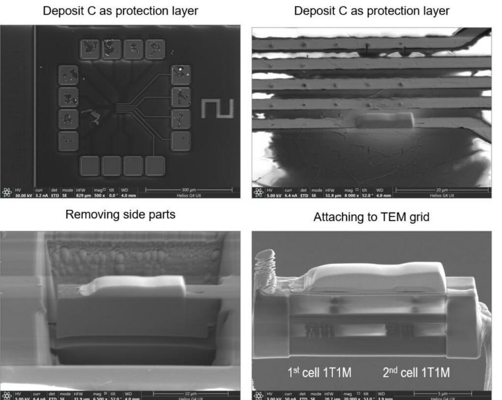
Researchers transfer a sheet of multilayer hexagonal boron nitride (h-BN) onto the back-end-of-line (BEOL) interconnections of silicon microchips containing CMOS transistors of the 180 nanometer node, and finalize the circuits by patterning the top electrodes and interconnections. The CMOS transistors provide outstanding control over the currents across the h-BN memristors, which allows us to achieve endurances of ~5 million cycles in memristors as small as ~0.053 square micron. They demonstrate in-memory computation by constructing logic gates, and measure spike-timing dependent plasticity (STDP) signals that are suitable for the implementation of spiking neural networks (SNN). The high performance and the relatively-high technology readiness level achieved represent a significant advance towards the integration of 2D materials in microelectronic products and memristive applications.
Communications Physics (2022) – Atomic-scale tuning of ultrathin memristors
Abstract
Continuous device downsizing and circuit complexity have motivated atomic-scale tuning of memristors. Herein, we report atomically tunable Pd/M1/M2/Al ultrathin (<2.5 nm M1/M2 bilayer oxide thickness) memristors using in vacuo atomic layer deposition by controlled insertion of MgO atomic layers into pristine Al2O3 atomic layer stacks guided by theory predicted Fermi energy lowering leading to a higher high state resistance (HRS) and a reduction of oxygen vacancy formation energy. Excitingly, memristors with HRS and on/off ratio increasing exponentially with M1/M2 thickness in the range 1.2–2.4 nm have been obtained, illustrating tunneling mechanism and tunable on/off ratio in the range of 10–10^4. Further dynamic tunability of on/off ratio by electric field is possible by designing of the atomic M2 layer and M1/M2 interface. This result probes ways in the design of memristors with atomically tunable performance parameters.
Introduction
Interest in neuromorphic computing has been steadily increasing in recent years, due to its potential to circumvent the Von Neumann bottleneck which arises from the extra energy and time required to transport data between memory and processor units during computation. Spearheaded by improvements in resistive random access memory (RRAM), researchers have attempted to mimic biological neuron and synapse operation by using artificial versions of these elements known as memristors. In memristors, the operations of both non-volatile memory storage and low-power computing are integrated in one device, taking advantage of the computing strengths of a neural system, namely pattern recognition and unstructured data sorting. RRAM may be used to implement multiple resistance states and thus serve as trainable synapses in neural networks. However, as the field of memristors, RRAM, and neuromorphic computing evolves, the ability to tune the memristive resistance, switching speed, cycling endurance, among other performance criteria, at the atomic scale will be important as device architectures evolve and potentially require devices with different performance capabilities closely integrated together. Control over these performance parameters of memristors at the atomic scale will become critically important to the success of neuromorphic computing.
Memristors are two-terminal devices typically consisting of an Ohmic and a Schottky electrode sandwiching a thin insulator, featuring a pinched hysteresis of resistance1 realized through the bipolar switching of two different serially connected resistors or a double-layer (M1/M2) dielectric oxide film. Alternatively, a unipolar memristor is normally comprised of two Schottky interfaces on either side of a thin insulator. The mobile species in the switching layer, typically oxygen vacancies (VO), can be driven back and forth in the M1/M2 film to create a conductive filament (CF). In this switching mechanism, a positive bias (SET) creates an electric field that in conjunction with joule heating causes VO from the vacancy rich M2 layer to diffuse through the higher quality dielectric M1 layer and form a CF, setting the memristor to the low resistance state (LRS). The opposite effect occurs when applying a negative voltage (RESET) and the CF is ruptured through VO diffusion and the memristor is reset to the high resistance state (HRS). Unipolar resistors experience the same CF formation to switch their resistance states, but SET and RESET may occur at both positive and negative bias voltages assisted by a compliance current.
Since the pioneering work by S. Williams in demonstration of the first Pt/TiO2/TiOx/Ti memristor, many dielectric materials have been studied for memristors using both physical vapor deposition (PVD) such as sputtering, evaporation, and chemical vapor deposition (CVD) such as atomic layer deposition (ALD). A myriad of metal-oxides have been utilized for their compatibility with common electrodes selected to form Ohmic and Schottky contacts, their CMOS compatibility, and their high level of performance in memristors. On/off (defined as HRS/LRS) ratios in the 10^2–10^3 range are acceptable for memristor operation, but many memristors have demonstrated higher on/off ratios up to 100,000 to 1 million. Some memristors have achieved switching speeds as low as ~100 ps, though typical memristors show switching speeds in the ~10 ns range, and low-power switching as low as 115 fJ34. The read/write endurance of the devices has also been observed as high as a trillion cycles.
In current memristors, VO are a part of many other defects present in the M1/M2 structure as the stack is often fabricated purposely as a “poor oxide” to facilitate CF formation. However, the lack of control of other unwanted defects has serious consequences such as electric leakage and charge traps that in turn impact memristor parameters including M1/M2 thickness, endurance, switching speed/power, on/off ratio, etc.
Conclusion
In conclusion, atomic-scale controlled VO doping of ultrathin pristine Al2O3 has been explored in this work by insertion of MgO atomic layers into Al2O3 atomic layer stacks grown using in vacuo ALD for atomically tunable memristors. Two effects of Mg doping in pristine Al2O3 are revealed in our DFT simulations: reduction of the Fermi energy and hence increase of the resistivity, and increased generation of VO, both desirable for high performance memristors. These two effects are both experimentally confirmed through a comparative study of memristor performance parameters with respect to the number and location of the inserted MgO atomic layers in the MgO/Al2O3 atomic layer stacks. Excitingly, this allows atomically tunable memristors to be achieved. Within the M1/M2 thickness of 1.2–2.4 nm, we show that the HRS can be tuned continuously over three orders of magnitude, leading to an on/off ratio tunable in the range of 10–10^4 in this thickness range. Furthermore, dynamically tunable on/off ratio by up to one order of magnitude was obtained by arranging the MgO atomic layers at the M1/M2 interface. Finally, an exponentially decreasing tunneling conductance with increasing M1/M2 thickness demonstrates that tunneling is the dominant HRS conduction mechanism of these memristors while the tunnel barrier height ET = Eb + Vsch is determined by the M1/M2 barrier height Eb and the Schottky barrier Vsch meaning that the Schottky and tunnel barriers work in tandem to limit current. In vacuo STS dI/dV characterization has revealed that higher Eb up to 1.45 eV can be obtained in less defective MgO/Al2O3 M1/M2 grown on Al electrode with a negligible metal–insulator interface, in contrast to much lower Eb 0.75 eV when a defective native oxide IL is present. Nevertheless, the Vsch of 1.19 eV can be maintained at the Pd/Al2O3 Schottky interface. This result shows a promising approach for design and fabrication of ultrathin memristors tunable at an atomic scale.

Brian Wang is a Futurist Thought Leader and a popular Science blogger with 1 million readers per month. His blog Nextbigfuture.com is ranked #1 Science News Blog. It covers many disruptive technology and trends including Space, Robotics, Artificial Intelligence, Medicine, Anti-aging Biotechnology, and Nanotechnology.
Known for identifying cutting edge technologies, he is currently a Co-Founder of a startup and fundraiser for high potential early-stage companies. He is the Head of Research for Allocations for deep technology investments and an Angel Investor at Space Angels.
A frequent speaker at corporations, he has been a TEDx speaker, a Singularity University speaker and guest at numerous interviews for radio and podcasts. He is open to public speaking and advising engagements.