

This is a follow up to my first article on programmable metallization cell memory in October, 2007
Best of all, the new technique can be used on existing, conventional storage which means that the cost will not be prohibitive.
“In using readily available materials, we’ve provided a way for this memory to be made at essentially zero extra cost, because the materials you need are already used in the chips—all you have to do is mix them in a slightly different way,” said Kozicki.
It might not be too long before we see products incorporating the new technology. Kozicki estimates that the first commercial product could be within 18 months. PMC has already attracted interest from several memory vendors, including Micron Technology. Samsung, Sony and IBM have also been interested in the technology.
Work then turned to silver-doped germanium sulfide electrolytes, and then finally to the current copper-doped germanium sulfide electrolytes. Axon Technologies has been licensing the basic concept since its formation in 2001. The first licensee was Micron Technology, who started work with PMC in 2002. Infineon followed in 2004, and a number of smaller companies have since joined as well.
Flash is based on the floating gate concept, essentially a modified transistor. Conventional transistors have three connections, the emitter, collector and base. The base is the essential component of the transistor, controlling the resistance between the emitter and collector, and thereby acting as a switch. In the floating gate transistor, the base is attached to a layer that traps electrons, leaving it switched on (or off) for extended periods of time. The floating gate can be re-written by passing a large current through the emitter-collector circuit.
It is this large current that is Flash’s primary drawback, and for a number of reasons. For one, each application of the current physically degrades the cell, and they will eventually not be able to be written to. Write cycles on the order of 10**5 to 10**6 are typical, limiting its application to roles where constant writing is not common. The current also requires an external circuit to generate, using a system known as a charge pump. The pump requires a fairly lengthy charging processes so writing is much slower than reading, and requires much more power as well. Flash is thus an “asymmetrical” system, much more so than conventional RAM or hard drives.
PMC, on the other hand, writes with relatively low power and high speeds. The speed is inversely related to the power applied (to a point, there are mechanical limits), so the performance can be tuned for different roles. Additionally, the writing process is “almost infinitely reversible”, making PMC much more universally applicable than Flash.
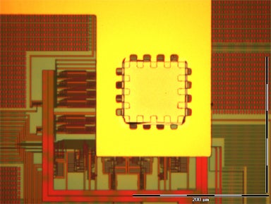
Three companies, Micron Technology, Qimonda and Adesto (a stealth-mode startup) have licensed the technology from Arizona State’s business spin-off, Axon Technologies. Kozicki says the first product containing the memory, a simple chip, is slated to come out in 18 months.
“No other technology can deliver the orders-of-magnitude improvement in power, performance and cost that this memory can,” says Narbeh Derhacobian, CEO of Adesto, who previously worked at AMD’s flash-memory division.
Adesto has received $6 million from Arch Venture Partners and additional funding from Harris & Harris, a venture firm specializing in nanotechnology.
Qimonda is a 13,500 employees computer memory company with over $4 billion/year in sales
FURTHER READING
Nano ionics defined: The term nanoionics is applied when electrochemical effects occur in materials and devices with interfaces, e.g., electrodes or electrochemically different material phases, that are closely-spaced (typically a few tens of nm or less). In this size regime, the functionality of ionic systems is quite different from the macro-scale versions but in a highly useful manner. For example, internal electric fields and ion mobilities are relatively high in nanoionic structures and this, combined with the short length scales, result in very fast response times. In addition, whereas deposition electrochemistry and most batteries use liquids or gels as ion transport media, nanoionics can take advantage of the fact that a variety of solid materials are excellent electrolytes, especially at the nanoscale.
The ability to redistribute metal mass within a structure via the application of a voltage leads to a wide range of potential applications. Electrodeposition of a noble metal such as silver will produce localized persistent but reversible changes to materials parameters and these changes can be used to control system behavior.
Examples of the applications of mass transport in solid electrolytes include the following:
-Electrical resistance changes radically when an electrodeposit with a resistivity in the tens of mW.cm or lower is deposited on or in a solid electrolyte which has a resistivity some eight orders of magnitude higher. This leads to a myriad of applications in solid state electronics, including memory, storage and logic.
-Deposition of mass can be used to alter the resonant frequency of a vibrating element in a microelectromechanical system (MEMS). This has applications in tunable high-Q MEMS-based resonators in RF systems.
-The optical properties of the electrodeposits have a profound effect on the transmission and reflection of light and so optical switches become a possibility using this technique. Such elements may be used in integrated optics and optical networks.
-The morphology of a typical electrodeposit leads to a large change in the wetting of a surface, making it highly hydrophobic, and so the technique can be used in microvalves and other fluid/droplet control devices in applications ranging from lab-on-a-chip to micro fuel cells.

Brian Wang is a Futurist Thought Leader and a popular Science blogger with 1 million readers per month. His blog Nextbigfuture.com is ranked #1 Science News Blog. It covers many disruptive technology and trends including Space, Robotics, Artificial Intelligence, Medicine, Anti-aging Biotechnology, and Nanotechnology.
Known for identifying cutting edge technologies, he is currently a Co-Founder of a startup and fundraiser for high potential early-stage companies. He is the Head of Research for Allocations for deep technology investments and an Angel Investor at Space Angels.
A frequent speaker at corporations, he has been a TEDx speaker, a Singularity University speaker and guest at numerous interviews for radio and podcasts. He is open to public speaking and advising engagements.