
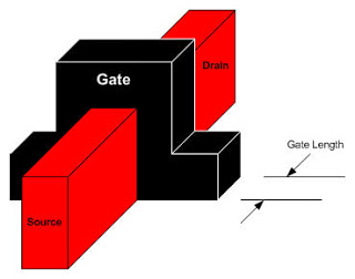

FinFET
Taiwan Semiconductor Manufacturing Co. is vying with Intel to become the first company to sell three-dimensional chips that boost the density of transistors in a single semiconductor by up to 1000 times. TSMC, the world’s largest contract chipmaker, could make its first 3DIC chips commercially available before the end of 2011. The timeframe for TSMC matches the end-2011 schedule that Intel has set for the launch of its 3D Tri-Gate chip. A 3DIC chip can achieve performance gains of about a third while consuming 50 percent less power. For this reason, 3DIC chips are particularly well suited to power new generations of mobile devices such as tablets and mobile phones.
“3D chips look more attractive because of their greater density,” Chiang said. “However, it is more difficult to make them because of the testing issues. If you have five stacked dies and one of the dies is bad, you have to scrap the whole thing.”
For this reason, TSMC is also developing so-called 2.5D chips that replace an organic polymer substrate with silicon to boost transistor density. Communications chipmaker Xilinx has contracted TSMC to make its Virtex-7 field programmable gate array (FPGA) using TSMC’s 2.5D chip technology that puts three chip dies on one silicon substrate. Xilinx said on March 8 that it expects the first samples of the Virtex-7 485T FPGA to be available by August.
FinFET versus Ultra Thin Body Silcon on Insulator
Chenming Hu, TSMC Distinguished Chair Professor of Microelectronics at University of California at Berkeley, provided a comparison of FinFET and Ultra Thin Body Silcon on Insulator (UTBSOI) Hu’s team developed the first UTBSOI FETs under the same 1996 DARPA contract that funded the first FinFET developments.

UTBSOI
We can scale the FETs at these smallest process nodes (14 or 22 nanometers), said Hu. We can, but there are just too many compromises. For example, Ioff (the off current) is too large. Vt, the FET threshold voltage, varies too much across a chip due to small variations in the gate length (Lg) and because dopant levels vary from transistor to transistor across a chip. When geometries as small, all you get are a handful of dopant atoms per transistor so even one dopant atom more or less creates parametric variations. The only way to overcome this variation is overdesign. Combating all of these problems increases design costs and forces Silicon Realization teams to run their designs with higher Vdd (to compensate for Vt variation), which drives up power consumption.
In 1996, Hu’s team developed two approaches to combating short-channel leakage. The first was the FinFET, which uses a 3D gate structure to make’s the FET gate much more effective by wrapping it around three sides of the channel instead of just one side. To do this, the FinFET’s channel is actually a raised structure—a fin. It no longer sits within the plane of the IC substrate.
The second way to trim the excess silicon from the channel is to fabricate the channel using an ultra-thin layer of silicon that sits on top of an insulator. Hu’s team built that structure too, under the same 1996 DARPA contract, and dubbed it UTBSOI (Ultra Thin Body Silcon on Insulator). The UTBSOI MOSFET simply has no deep silicon for the drain to affect. It’s been eliminated by using the thin silicon film to build the channel.
It only takes one extra mask to create the silicon fin. The FinFET manufacturing process is entirely compatible with contemporary advanced CMOS manufacturing and production techniques. No new magic required. After the fin is constructed, the rest of the processing is essentially planar because the fin just isn’t that tall. Fin height is on the order of 30nm for a fin that’s 20nm thick. After that, said Hu, it’s easy to scale the FETs. Just make the fin thinner and everything else just sort of falls out.
How thin can the FinFET fins get? Hu noted that a university team at KAIST (Korea Advanced Institute of Science and Technology) successfully built 3nm FinFETs using e-beam lithography five years ago in 2006. (I actually wrote about this achievement in the preface to chapter 15 of my book “Designing SOCs with Configured Cores” back in 2006.) However, making one such FinFET is a far cry from production noted Hu. Even so, Hu predicted that Intel would be able to push its Tri-Gate technology below 10nm.
There are also important differences between FinFETs and UTBSOI.
In UTBSOI’s favor, it’s relatively easy to add back biasing under the channel and beneath the insulating layer, if that’s desired. There’s no easy way to add back biasing to FinFETs without cutting the gate in two but you could do it.
The biggest difference, said Hu, is which entity is responsible to controlling the key FET parameters. For FinFETs, the key metric is the ratio of fin thickness to gate length. Both of these dimensions rely solely on the lithographic and etching processes and both of those are under the fab’s control. For UTBSOI, the key metric is the ratio of the channel thickness to the gate length and Soitec is largely responsible for controlling the film thickness in the wafers supplied to the fab. Consequently, said Hu, UTBSOI may be ready for production sooner but FinFETs have better long-term scalability.
Looking to the immediate future, Hu says here’s what will likely happen. Intel will use FinFETs in its 22nm manufacturing process and may well be able to continue using them “beyond 10nm.” Meanwhile, other semiconductor manufacturers and foundries may use UTBSOI for 22nm or 18nm processes to gain market share or protect existing market share.
“Competition will bring out the best in both” approaches, said Hu.
If you liked this article, please give it a quick review on ycombinator or StumbleUpon. Thanks

Brian Wang is a Futurist Thought Leader and a popular Science blogger with 1 million readers per month. His blog Nextbigfuture.com is ranked #1 Science News Blog. It covers many disruptive technology and trends including Space, Robotics, Artificial Intelligence, Medicine, Anti-aging Biotechnology, and Nanotechnology.
Known for identifying cutting edge technologies, he is currently a Co-Founder of a startup and fundraiser for high potential early-stage companies. He is the Head of Research for Allocations for deep technology investments and an Angel Investor at Space Angels.
A frequent speaker at corporations, he has been a TEDx speaker, a Singularity University speaker and guest at numerous interviews for radio and podcasts. He is open to public speaking and advising engagements.