

Ad Support : Nano Technology Netbook Technology News Computer Software
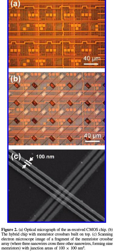
Hybrid reconfigurable logic circuits were fabricated by integrating memristor-based crossbars onto a foundry-built CMOS (complementary
metal-oxide-semiconductor) platform using nanoimprint lithography, as well as materials and processes that were compatible with the
CMOS. Titanium dioxide thin-film memristors served as the configuration bits and switches in a data routing network and were connected to
gate-level CMOS components that acted as logic elements, in a manner similar to a field programmable gate array. We analyzed the chips
using a purpose-built testing system, and demonstrated the ability to configure individual devices, use them to wire up various logic gates
and a flip-flop, and then reconfigure devices.
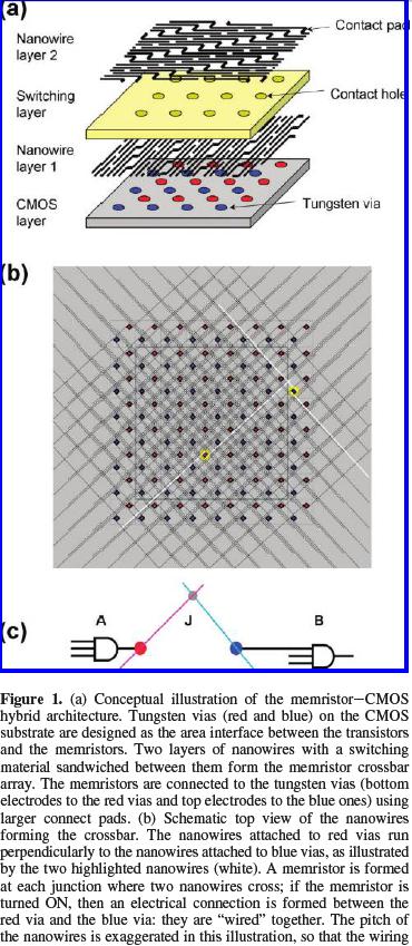
One possible way to extend Moore’s law beyond the limits of transistor scaling is to obtain the equivalent circuit functionality using fewer devices or components, i.e., get more computing per transistor on a chip. One proposal for achieving this end was the hybrid CMOL (CMOS/molecule) architecture of Strukov and Lihkarev, which was modified by two of us to improve its manufacturability and separate the routing and computing functions; this was called FPNI (field-programmable nanowire interconnect). Rather than relentlessly shrinking transistor sizes, FPNI separates the logic elements from the data routing network by lifting the configuration bits, routing switches, and associated components out of the CMOS layer and making them a part of the interconnect. Memristor cross bars can be fabricated directly above the CMOS circuits, and serve as the reconfigurable data routing network. A 2D array of vias provides electrical connectivity between the CMOS and the memristor layer. Memristors are ideal for this FPGA-like application because a single device is capable of realizing functions that need several transistors in a CMOS circuit, namely, a configuration-bit flip-flop and associated data-routing multiplexer. A further advantage is that their memory function is nonvolatile, which means they do not require power to refresh their states, even if the power to the chip is turned off completely. Numerical
simulations showed that this type of architecture can dramatically increase the logic density of an FPGA-like chip without degrading power dissipation or speed even in the presence of large numbers (up to 20%) of defective components.
2. Towards Memristor-CMOS-Hybrid Semiconductor Devices for Neural Networks
One of the key issues for implementing neural networks on semiconductor integrated circuits is “how we implement non-volatile analog synapses”. Obviously this becomes critical if the network requires learning rules, i.e., the synaptic weights must be preserved and be updated according to the rules. Many engineers have tried to design analog synaptic devices based on existing flash-memory technologies, but they had difficulties in designing associate controllers for electron injection and ejection as well as increasing the limited frequency of the rewriting. Recently so-called “memristor” which is the fourth basic circuit element originally introduced by Leon Chua in 1971, has been re-spotlighted since Strukov et al. presented the equivalent physical examples. Memristive devices could naturally be exploited for implementing non-volatile synapses on electronic circuits because they are equivalent to resistors whose resistances can be held or modulated by the amount of the integrated current of them.
3. Nanoletters – Nanoscale Memristor Device as Synapse in Neuromorphic Systems
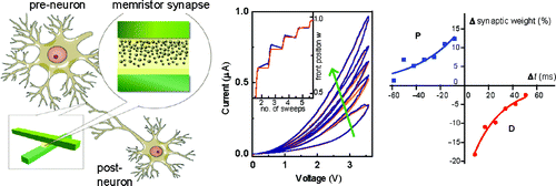
A memristor is a two-terminal electronic device whose conductance can be precisely modulated by charge or flux through it. Here we experimentally demonstrate a nanoscale silicon-based memristor device and show that a hybrid system composed of complementary metal−oxide semiconductor neurons and memristor synapses can support important synaptic functions such as spike timing dependent plasticity. Using memristors as synapses in neuromorphic circuits can potentially offer both high connectivity and high density required for efficient computing.
Supporting information for Nanoscale Memristor Device as Synapse in Neuromorphic Systems (7 pages)
4. A memristor is the fourth fundamental circuit element (resistor, capacitor, and inductor being the three other well-known circuit elements) that can be described using two equations: a quasi-static equation, and a dynamical equation. The memristor’s properties, Williams explained, depend on time; the state variable depends on the device’s past history. The consequences of these properties and characteristics are that the device’s C-V characteristic curve is a pinched hysteresis loop; the voltage and current always have to be 0 at the same time, so the device cannot store charge or energy, but it can store information. “This is key and profound in terms of being able to build new types of electronic circuits,” observed Williams.
The reason memristors join the familiar LCR elements as fundamental is because no combination of LCR circuit elements can be put together to obtain an equivalent circuit that achieves the C-V characteristic curve of the memristor. “These set of four devices (L, C, R and the memristor) form a complete set of functions that can be used to synthesize a wide variety of functions for electronics circuits,” explained Williams. Circuit designers have had to build circuits without memristors, but it required a lot of transistors — “It takes an equivalent circuit made up of 15 transistors and 3 capacitors to emulate a single memristor,” he noted. With a true memristor, electronic circuitry can be greatly simplified, he explained — essentially decreasing the transistor count by a significant fraction, and in some circuits maybe by an order-of-magnitude. “That’s an interesting way of moving Moore’s Law forward,” he observed — “not by getting more functionality by making the transistor smaller, but getting the same functionality by using fewer transistors to achieve the same ends.”
HP has now developed a device that can be operated as either a memristor or a memistor, depending on whether or not it is operated as a 2-terminal or a 3-terminal device (based on how the bias voltage is applied). The device itself is a 30nm wide (5nm active region) single structure that can be utilized as three different memristors when operated as a 2-terminal device, or operated as a single 3-terminal memistor. Results will be published soon, Williams promised, with the intentions to be able to build analog computers someday.
Williams’ research group has built a hybrid CMOS-memristor chip — using an inkjet CMOS process at a foundry that makes HP inkjet technology — developing all the processing techniques required to integrate memristors and memistors with transistors in a circuit. “From this platform, we hope to launch a number of new technologies for memory” (e.g., replacing flash memory storage), “and when we get giddy, we hope to replace DRAM, SRAM, magnetic card disks, DVDs, CDs, and so forth,” said Williams. “We’re also looking at doing away with Boolean logic — i.e., using synaptic computing,” based on the analog difference in the junctions of the device. The challenge, he said, is to monitor the processes in the region between the conducting channel and the top electrode, essentially watching switching in real time.
The aforementioned hybrid CMOS-memristor had 100nm memristor features, but the intent of using the inkjet process was to demonstrate the process compatibility as well as to show that different generations of feature sizes could be used with respect to CMOS and the memristors, Williams pointed out. “What we’re looking to do is to continually shrink memristors to smaller and smaller sizes long after people stop trying to shrink CMOS,” he said. “We think that you can make very capable circuits with 45nm CMOS for example, but then integrate maybe even 5nm memristors on top of that — a combination that is very interesting for both storage and computation.”
Supporting Advertising
Trading Futures
Nano Technology
Netbook Technology News
Computer Software
Future Predictions
Thank You

Brian Wang is a Futurist Thought Leader and a popular Science blogger with 1 million readers per month. His blog Nextbigfuture.com is ranked #1 Science News Blog. It covers many disruptive technology and trends including Space, Robotics, Artificial Intelligence, Medicine, Anti-aging Biotechnology, and Nanotechnology.
Known for identifying cutting edge technologies, he is currently a Co-Founder of a startup and fundraiser for high potential early-stage companies. He is the Head of Research for Allocations for deep technology investments and an Angel Investor at Space Angels.
A frequent speaker at corporations, he has been a TEDx speaker, a Singularity University speaker and guest at numerous interviews for radio and podcasts. He is open to public speaking and advising engagements.