

The elimination of sawing kerf loss combined with its ability to make thinner wafers of high quality make the implant-cleave wafering approach technically and economically attractive. For example, while a typical silicon usage to make a solar wafer including kerf loss is approaching 6g/W, the new implant-cleave process consumes merely 2.5g/W at its highest thickness of 150µm. Using $50/kg for the price of polysilicon, this corresponds to a 60% cost savings in silicon material. Higher savings occur when the new method’s unique ability to make thinner wafers is utilized.
Comparison of fracture forces for wet chemical etched wafers.
        Thickness (µm)  Fracture force (N)

Wiresaw     230          28.6

PolyMax      85          43.0

PolyMax     100          59.7
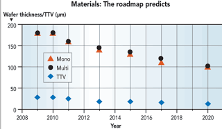
The new wafering method cleaves rather than saws, and this fundamentally affects the amount of variation in wafer thickness and roughness during the manufacturing process. Not only are the variations much smaller than wafers that have been wire sawed, the implant and cleave physics cause a linear coupling between these variations and the wafer thickness. For example, a 150µm PolyMax as-cleaved wafer will typically have a variation of +/- 2µm and RMS roughness of 0.4µm, but a 20µm PolyMax wafer will show thickness variation of less than +/- 0.2µm and RMS roughness of 0.06µm. This strong thickness-variation interdependence is what enables the method’s ultra-thin thickness roadmap
During the first step, a high energy hydrogen (proton) beam irradiates the top surface of silicon bricks or ingots. The incident mono-energetic protons lose their energy as they traverse into the silicon material and come to rest at a pre-determined depth to form a stressed cleave layer. The silicon wafer thickness is thus accurately determined by the depth or range of the implanted protons, which in turn is controlled by the energy of the proton beam. Implant energies of 1-4MeV are required to fabricate silicon wafers of 20µm-150µm in thickness suitable for solar photovoltaic use. For example, a 2MeV implant will produce a 50µm wafer, while a 3MeV implant will yield 85µm wafers. During a single implant run, a total of 36, 156mm x 156mm bricks (6×6 array) or 64, 125mm x 125mm single crystal silicon bricks (8×8 array) are batch processed for high-volume manufacturing.
During the second step, the implanted silicon brick is induced to fracture, or cleave, in a highly controlled manner along the implanted ion stress layer. A single wafer of silicon is detached from each brick and the process is subsequently repeated on the newly exposed brick surface. Repeating implant and cleave cycles will thus convert a silicon brick to its equivalent thickness of wafers. As opposed to using wire-saws, the cleaving technique essentially eliminates expensive silicon material waste due to kerf loss.
The material properties of the wafers produced by the new implant-cleave approach discussed above were presented and compared to traditional wire-sawn wafers. With its ability to enable wafer manufacturing of 20µm to 150µm thickness without kerf loss, the new method is positioned to emerge as a low cost high quality wafering approach supporting the fast growing crystalline silicon PV market.
If you liked this article, please give it a quick review on ycombinator or StumbleUpon. Thanks

Brian Wang is a Futurist Thought Leader and a popular Science blogger with 1 million readers per month. His blog Nextbigfuture.com is ranked #1 Science News Blog. It covers many disruptive technology and trends including Space, Robotics, Artificial Intelligence, Medicine, Anti-aging Biotechnology, and Nanotechnology.
Known for identifying cutting edge technologies, he is currently a Co-Founder of a startup and fundraiser for high potential early-stage companies. He is the Head of Research for Allocations for deep technology investments and an Angel Investor at Space Angels.
A frequent speaker at corporations, he has been a TEDx speaker, a Singularity University speaker and guest at numerous interviews for radio and podcasts. He is open to public speaking and advising engagements.
Truly a space-age process. Changes cutting from edge-accessed to face-accessed. But the disadvantages are power/area and time tying up an expensive machine. Can you tell us anything about the implant-dose required?