
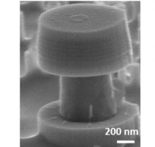
Researchers designed subwavelength micro-disk lasers (MDLs) as small as 1μm in diameter on exact (001) silicon, using colloidal lithography (dispersing silica colloidal beads as hard masks before etching the prepared QD material layers). Micron sized lasers are 1,000 times shorter in length, and 1 million times smaller than current onchip lasers.

A group of scientists from Hong Kong University of Science and Technology; the University of California, Santa Barbara; Sandia National Laboratories and Harvard University were able to fabricate tiny lasers directly on silicon — a huge breakthrough for the semiconductor industry and well beyond.
For more than 30 years, the crystal lattice of silicon and of typical laser materials could not match up, making it impossible to integrate the two materials — until now.
They integrated subwavelength cavities — the essential building blocks of their tiny lasers — onto silicon enabled them to create and demonstrate high-density on-chip light-emitting elements.
To do this, they first had to resolve silicon crystal lattice defects to a point where the cavities were essentially equivalent to those grown on lattice-matched gallium arsenide (GaAs) substrates. Nano-patterns created on silicon to confine the defects made the GaAs-on-silicon template nearly defect free and quantum confinement of electrons within quantum dots grown on this template made lasing possible.
The group was then able to use optical pumping, a process in which light, rather than electrical current, “pumps” electrons from a lower energy level in an atom or molecule to a higher level, to show that the devices work as lasers.
“Putting lasers on microprocessors boosts their capabilities and allows them to run at much lower powers, which is a big step toward photonics and electronics integration on the silicon platform,” said professor Kei May Lau, Department of Electronic and Computer Engineering, Hong Kong University of Science and Technology.
Traditionally, the lasers used for commercial applications are quite large — typically 1 mm x 1 mm. Smaller lasers tend to suffer from large mirror loss.
But the scientists were able to overcome this issue with “tiny whispering gallery mode lasers — only 1 micron in diameter — that are 1,000 times shorter in length, and 1 million times smaller in area than those currently used,” said Lau.
Whispering gallery mode lasers are considered an extremely attractive light source for on-chip optical communications, data processing and chemical sensing applications.
“Our lasers have very low threshold and match the sizes needed to integrate them onto a microprocessor,” Lau pointed out. “And these tiny high-performance lasers can be grown directly on silicon wafers, which is what most integrated circuits (semiconductor chips) are fabricated with.”
In terms of applications, the group’s tiny lasers on silicon are ideally suited for high-speed data communications.
“Photonics is the most energy-efficient and cost-effective method to transmit large volumes of data over long distances. Until now, laser light sources for such applications were ‘off chip’ — missing — from the component,” Lau explained. “Our work enables on-chip integration of lasers, an [indispensable] component, with other silicon photonics and microprocessors.”
The researchers expect to see this technology emerge in the market within 10 years.
Next, the group is “working on electrically pumped lasers using standard microelectronics technology,” Lau said.
Abstract
Subwavelength micro-disk lasers (MDLs) as small as 1 μm in diameter on exact (001) silicon were fabricated using colloidal lithography. The micro-cavity gain medium incorporating five-stacked InAs quantum dot layers was grown on a high crystalline quality GaAs-on-V-grooved-Si template with no absorptive intermediate buffers. Under continuous-wave optical pumping, the MDLs on silicon exhibit lasing in the 1.2-μm wavelength range with low thresholds down to 35 μW at 10 K. The MDLs compare favorably with devices fabricated on native GaAs substrates and state-of-the-art work reported elsewhere. Feasibility of device miniaturization can be projected by size-dependent lasing characteristics. The results show a promising path towards dense integration of photonic components on the mainstream complementary metal–oxide–semiconductor platform.
SOURCES- Applied Physics Letters, Hong Kong University of Science and Technology; the University of California, Santa Barbara; Sandia National Labs, Analog EEtimes

Brian Wang is a Futurist Thought Leader and a popular Science blogger with 1 million readers per month. His blog Nextbigfuture.com is ranked #1 Science News Blog. It covers many disruptive technology and trends including Space, Robotics, Artificial Intelligence, Medicine, Anti-aging Biotechnology, and Nanotechnology.
Known for identifying cutting edge technologies, he is currently a Co-Founder of a startup and fundraiser for high potential early-stage companies. He is the Head of Research for Allocations for deep technology investments and an Angel Investor at Space Angels.
A frequent speaker at corporations, he has been a TEDx speaker, a Singularity University speaker and guest at numerous interviews for radio and podcasts. He is open to public speaking and advising engagements.