
In an advance that helps pave the way for next-generation electronics and computing technologies—and possibly paper-thin gadgets —scientists with the U.S. Department of Energy’s Lawrence Berkeley National Laboratory (Berkeley Lab) developed a way to chemically assemble transistors and circuits that are only a few atoms thick.
What’s more, their method yields functional structures at a scale large enough to begin thinking about real-world applications and commercial scalability.

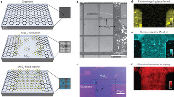
Growth scheme and optical characterizations of the graphene–MoS2 heterostructure.
Nature Nanotechnology – Large-scale chemical assembly of atomically thin transistors and circuits
The scientists controlled the synthesis of a transistor in which narrow channels were etched onto conducting graphene, and a semiconducting material called a transition-metal dichalcogenide, or TMDC, was seeded in the blank channels. Both of these materials are single-layered crystals and atomically thin, so the two-part assembly yielded electronic structures that are essentially two-dimensional. In addition, the synthesis is able to cover an area a few centimeters long and a few millimeters wide.
“This is a big step toward a scalable and repeatable way to build atomically thin electronics or pack more computing power in a smaller area,” says Xiang Zhang, a senior scientist in Berkeley Lab’s Materials Sciences Division who led the study.
Zhang also holds the Ernest S. Kuh Endowed Chair at the University of California (UC) Berkeley and is a member of the Kavli Energy NanoSciences Institute at Berkeley. Other scientists who contributed to the research include Mervin Zhao, Yu Ye, Yang Xia, Hanyu Zhu, Siqi Wang, and Yuan Wang from UC Berkeley as well as Yimo Han and David Muller from Cornell University.
Their work is part of a new wave of research aimed at keeping pace with Moore’s Law, which holds that the number of transistors in an integrated circuit doubles approximately every two years. In order to keep this pace, scientists predict that integrated electronics will soon require transistors that measure less than ten nanometers in length.
Transistors are electronic switches, so they need to be able to turn on and off, which is a characteristic of semiconductors. However, at the nanometer scale, silicon transistors likely won’t be a good option. That’s because silicon is a bulk material, and as electronics made from silicon become smaller and smaller, their performance as switches dramatically decreases, which is a major roadblock for future electronics.
Researchers have looked to two-dimensional crystals that are only one molecule thick as alternative materials to keep up with Moore’s Law. These crystals aren’t subject to the constraints of silicon.
In this vein, the Berkeley Lab scientists developed a way to seed a single-layered semiconductor, in this case the TMDC molybdenum disulfide (MoS2), into channels lithographically etched within a sheet of conducting graphene. The two atomic sheets meet to form nanometer-scale junctions that enable graphene to efficiently inject current into the MoS2. These junctions make atomically thin transistors.
“This approach allows for the chemical assembly of electronic circuits, using two-dimensional materials, which show improved performance compared to using traditional metals to inject current into TMDCs,” says Mervin Zhao, a lead author and Ph.D. student in Zhang’s group at Berkeley Lab and UC Berkeley.
Optical and electron microscopy images, and spectroscopic mapping, confirmed various aspects related to the successful formation and functionality of the two-dimensional transistors.
In addition, the scientists demonstrated the applicability of the structure by assembling it into the logic circuitry of an inverter. This further underscores the technology’s ability to lay the foundation for a chemically assembled atomic computer, the scientists say.
“Both of these two-dimensional crystals have been synthesized in the wafer scale in a way that is compatible with current semiconductor manufacturing. By integrating our technique with other growth systems, it’s possible that future computing can be done completely with atomically thin crystals,” says Zhao.
Abstract
Next-generation electronics calls for new materials beyond silicon, aiming at increased functionality, performance and scaling in integrated circuits. In this respect, two-dimensional gapless graphene and semiconducting transition-metal dichalcogenides have emerged as promising candidates due to their atomic thickness and chemical stability. However, difficulties with precise spatial control during their assembly currently impede actual integration into devices. Here, we report on the large-scale, spatially controlled synthesis of heterostructures made of single-layer semiconducting molybdenum disulfide contacting conductive graphene. Transmission electron microscopy studies reveal that the single-layer molybdenum disulfide nucleates at the graphene edges. We demonstrate that such chemically assembled atomic transistors exhibit high transconductance (10 µS), on–off ratio (∼10^6) and mobility (∼17 cm2 V−1 s−1). The precise site selectivity from atomically thin conducting and semiconducting crystals enables us to exploit these heterostructures to assemble two-dimensional logic circuits, such as an NMOS inverter with high voltage gain (up to 70).
15 pages of supplemental information
SOURCES – Berkeley Labs, Nature Nanotechnology

Brian Wang is a Futurist Thought Leader and a popular Science blogger with 1 million readers per month. His blog Nextbigfuture.com is ranked #1 Science News Blog. It covers many disruptive technology and trends including Space, Robotics, Artificial Intelligence, Medicine, Anti-aging Biotechnology, and Nanotechnology.
Known for identifying cutting edge technologies, he is currently a Co-Founder of a startup and fundraiser for high potential early-stage companies. He is the Head of Research for Allocations for deep technology investments and an Angel Investor at Space Angels.
A frequent speaker at corporations, he has been a TEDx speaker, a Singularity University speaker and guest at numerous interviews for radio and podcasts. He is open to public speaking and advising engagements.