
For CMOS logic transistors, when we approach the direct source-drain tunneling limit, we could move to recessed channel devices and use channel lengths longer than the minimum feature size. This could allow us to continue miniaturization and increase component density. For example, at the 5nm node, we could have a 8nm channel length transistor without sacrificing density. Recessed channel devices also enable us to address issues with short channel effects such as Drain Induced Barrier Lowering (DIBL). Furthermore, moving to recessed channel devices could enable easy implementation of Monolithic 3D-ICs. See this page for more details. Next-generation logic transistors such as Finfets can be constructed with recessed channel topologies too. Hynix has done a lot of work on recessed channel Finfets for DRAM. Other high-density device structures where channel length is longer than the minimum feature size exist, such as vertical transistors. These are being actively explored by the DRAM industry too.
Conclusion: It certainly looks like we might be able to miniaturize CMOS technologies beyond the 5nm node someday.
Memristors can be fashioned into non-volatile solid-state memory, which would allow greater data density than hard drives with access times potentially similar to DRAM, replacing both components. HP prototyped a crossbar latch memory using the devices that can fit 100 gigabits in a square centimeter, and has designed a highly scalable 3D design (consisting of up to 1000 layers or 1 petabit per cm3). HP has reported that its version of the memristor is currently about one-tenth the speed of DRAM. The devices’ resistance would be read with alternating current so that the stored value would not be affected.
So CMOS transistors could be replaced before they hit their fundamental limits.
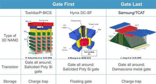
The NAND flash industry has monolithic 3D on their roadmap in the next 2-3 years.
If you liked this article, please give it a quick review on ycombinator or StumbleUpon. Thanks

Brian Wang is a Futurist Thought Leader and a popular Science blogger with 1 million readers per month. His blog Nextbigfuture.com is ranked #1 Science News Blog. It covers many disruptive technology and trends including Space, Robotics, Artificial Intelligence, Medicine, Anti-aging Biotechnology, and Nanotechnology.
Known for identifying cutting edge technologies, he is currently a Co-Founder of a startup and fundraiser for high potential early-stage companies. He is the Head of Research for Allocations for deep technology investments and an Angel Investor at Space Angels.
A frequent speaker at corporations, he has been a TEDx speaker, a Singularity University speaker and guest at numerous interviews for radio and podcasts. He is open to public speaking and advising engagements.