

Metalenses have been used to image microscopic features of tissue and resolve details smaller than a wavelength of light. Now, Harvard researchers have turned the metalens towards space.
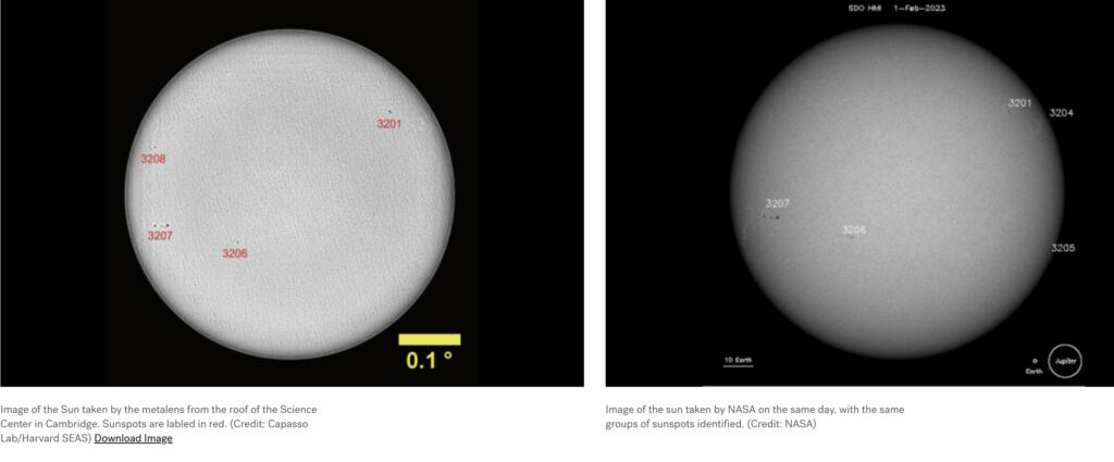
Researchers at the Harvard John A. Paulson School of Engineering and Applied Sciences (SEAS) have developed a 10-centimeter-diameter glass metalens that can image the sun, the moon and distant nebulae with high resolution. It is the first all-glass, large-scale metalens in the visible wavelength that can be mass produced using conventional CMOS fabrication technology.
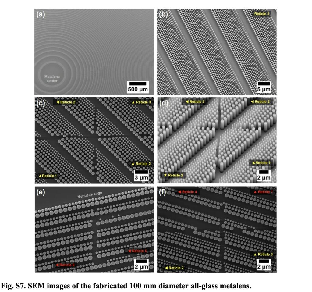
Park and the team developed a technique to stitch together several patterns of nanopillars using the DUV projection lithography tool. By dividing the lens into 25 sections but using only the 7 sections of a quadrant considering the rotational symmetry, the researchers showed that DUV projection lithography could pattern 18.7 billion designed nanostructures onto a 10-centimeter circular area in a matter of minutes. The team also developed a vertical glass etching technique that allows the creation of high-aspect ratio, smooth-sidewall nanopillars etched into glass.


“Using the same DUV projection lithography, one could produce large-diameter, aberration-correcting meta-optics or even larger lenses on larger glass diameter wafers as the corresponding CMOS foundry tools become increasingly available in the industry,” said Soon Wei Daniel Lim, a postdoctoral fellow at SEAS and co-first author of the paper.
All-Glass 100 mm Diameter Visible Metalens for Imaging the Cosmos
Metasurfaces, optics made from subwavelength-scale nanostructures, have been limited to millimeter-sizes by the scaling challenge of producing vast numbers of precisely engineered elements over a large area. In this study, researchers demonstrate an all-glass 100 mm diameter metasurface lens (metalens) comprising 18.7 billion nanostructures that operates in the visible spectrum with a fast f-number (f/1.5, NA = 0.32) using deep-ultraviolet (DUV) projection lithography. the work overcomes the exposure area constraints of lithography tools and demonstrates that large metasurfaces are commercially feasible. Additionally, we investigate the impact of various fabrication errors on the imaging quality of the metalens, several of which are specific to such large area metasurfaces. They demonstrate direct astronomical imaging of the Sun, the Moon, and emission nebulae at visible wavelengths and validate the robustness of such metasurfaces under extreme environmental thermal swings for space applications.
Most flat metalenses, which use millions of pillar-like nanostructures to focus light, are about the size of a piece of glitter. In 2019, Capasso and his team developed a centimeter-scale metalens using a technique called deep-ultraviolet (DUV) projection lithography, which projects and forms a nanostructure pattern that can be directly etched into the glass wafer, eliminating the time-consuming writing and deposition processes that were required for previous metalenses.
DUV projection lithography is commonly used to pattern fine lines and shapes in silicon chips for smartphones and computers. Joon-Suh Park, a former graduate student at SEAS and current postdoctoral fellow in Capasso’s team, demonstrated that the technique could not only be used to mass produce metalenses but also increase their size for applications in virtual and augmented reality.
But making the metalens even larger for applications in astronomy and free-space optical communications posed an engineering problem.
In early 2023, there was demonstration of a 10cm (~4in) planar metalens, which was a world record in size for a visible spectrum metalens. This metalens technology, developed by Harvard University, is enabling for technologies such as UAS imaging systems with five optical elements to be replaced with only three elements resulting in either 4x enhancement in resolution for the same SWaP of existing systems or 10x enchantment in SWaP for the same resolution.
Metalenses have been used to image microscopic features of tissue and resolve details smaller than a wavelength of light. Now, #hseas researchers have turned the metalens towards the cosmos. https://t.co/DEJS0EBznv
— Harvard SEAS (@hseas) January 17, 2024

Brian Wang is a Futurist Thought Leader and a popular Science blogger with 1 million readers per month. His blog Nextbigfuture.com is ranked #1 Science News Blog. It covers many disruptive technology and trends including Space, Robotics, Artificial Intelligence, Medicine, Anti-aging Biotechnology, and Nanotechnology.
Known for identifying cutting edge technologies, he is currently a Co-Founder of a startup and fundraiser for high potential early-stage companies. He is the Head of Research for Allocations for deep technology investments and an Angel Investor at Space Angels.
A frequent speaker at corporations, he has been a TEDx speaker, a Singularity University speaker and guest at numerous interviews for radio and podcasts. He is open to public speaking and advising engagements.
what is the current cost of a cmos foundry tool? Is there a market for used tools? Lithography using deep ultraviolet rays seems specialized and expensive, but I have no idea.
I’m trying to figure out if these scientists have access to a foundry or if they just prototyped the metalens. If a foundry were set up to manufacture millions of larger metalenses, what would be the addressable market?
Neat technology. Interested to see where it could be used on a mass scale.
While the authors are getting all warm-and-fuzzy with numerical apertures, giga-arrays of nanostructures, genetic algorithms and (I’m frankly surprised they missed mentioning) A.I., use your own eyeballs and look at the picture.
I have an old fashioned DSLR camera. If there are smudges on the attached lens, I know that the image — no matter how well focussed — will be blurry. Smudges, bad. Perfectly clear lens without lil’ bits of dust and leftover lunch attached.
Those lenses are FAR from “optically clear”. I imagine that while images of The Sun, or planetary nebulæ could be focussed, the signal-to-noise ratio, or the amount of smudginess… is pretty high.
________________________________________
Rightly, the authors imagine SPACE based deployment of these things. Weight, and the extraordinary penalty for lofting heavy things aboard spacecraft. As-light-as-possible is the usual engineering directive. Thus, for little light-sail propelled telescopic probes, these metalens plates might be absolutely The Thing to implement.
Noise — smudge noise — can certainly be processed out with fancy Photoshop™ type processing. But having near-zero mass is BIG.
Various proposals envision powerful photonic sails that take such probes out to the Kuiper and Oört belts, at the least. Some envision getting all the way to our nearer neighborhood stars. REALLY low mass is key, even if the tradeoff is smudginess.
⋅-⋅-⋅ Just saying, ⋅-⋅-⋅
⋅-=≡ GoatGuy ✓ ≡=-⋅
While the image quality coming off of it is certainly not on par with conventional camera optics, it’s not hot garbage either. At f/1.5, and an aperture of 100mm, that means this is a 150mm focal length lens, and f/1.5 is incredibly bright for a lens that long. Combined with the fact that it basically weighs nothing and was produced in a matter of minutes, we may see a revolution of cheap, lightweight and arbitrarily bright and long lenses for cameras in the future, if the technology improves to provide better image quality. The biggest issues with large lenses is that they take large amounts of heavy glass and days of grinding work, sometimes by hand, leading to extremely high prices. This metalens solves everything.
Smaller than a wavelength of light. Radio waves? Short waves? Millimeter waves? Speak to me in Angstroms.
Smaller than a wavelength of visible light. 400 nm is visible wavelength and that’s 4000 angstroms.