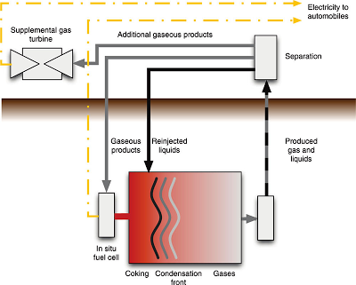
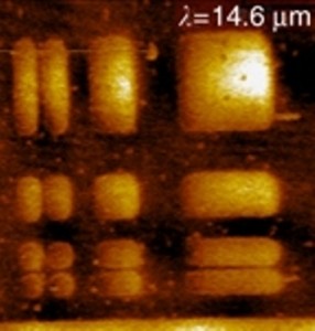
A silicon chip with integrated laser and optical grating offers new possibilities for telecommunications

An ark-shaped diffraction grating is used to selectively reflect light from a laser back into the device. The photo also shows the waveguides used to channel light back and forth. Copyright : A*STAR Research Silicon is an ideal platform for integrated photonic circuits because the material is cheap and readily available. Silicon chips with an …

Read more

Growing ‘Epidemic’ of Heart Attacks, Strokes, Cancer, Diabetes Threatens China’s Economic and Social Well-Being

The World Bank reports that based on current trends, the Chinese can expect to live only 66 “healthy years” (years free from disease and disability), ten years less than in some leading G-20 countries Non-communicable chronic diseases (NCDs) are the leading cause of death in China, accounting for close to 70 percent of the disease …

Read more

Heim Theory Falsified

Heim theory is a physics theory, initially proposed by a German physicist, the late Burkhard Heim, that attempts to develop a theory of everything. Heim theory’s six dimensional model was later extended to eight and twelve dimensions, in collaboration with W. Dröscher. Walter Dröscher and Jochem Häuser have attempted to apply it to nonconventional space …

Read more

Building New Materials from Synthetically Modified Proteins

Matthew Francis, PhD, Rising star of nanotech at UC-Berkeley 10:15-10:45am Building New Materials from Synthetically Modified Proteins Protein desirable properties – Rigid three dimensional structures for object positioning self assembled capabiliities to establish order over large lengths dynamic shape changes in response to external stimuli analyte binding with high specificity Lab working on site selective …

Read more

Graphene optical modulators could lead to 500 Gigahertz communications

Shown is a scanning electron microscope (SEM) image magnifying the key structures of the graphene-based optical modulator. (Colors were added to enhance the contrast). Gold (Au) and platinum (Pt) electrodes are used to apply electrical charges to the sheet of graphene, shown in blue, placed on top of the silicon (Si) waveguide, shown in red. …

Read more

Revolutionary new paper computer shows flexible future for smartphones and tablets

Professor Roel Vertegaal’s PaperPhone is best described as a flexible iPhone. The world’s first interactive paper computer is set to revolutionize the world of interactive computing. “This is the future. Everything is going to look and feel like this within five years,” says creator Roel Vertegaal, the director of Queen’s University Human Media Lab,. “This …

Read more

Fuel Cell Electricity production with in situ carbon capture can reduce CO2 from oil shale energy 3 times lower

A team at Stanford University is proposing using solid oxide fuel cells as the basis for a method for electricity production from oil shale with in situ carbon capture (EPICC) as a means to provide transportation services from oil shale with greatly reduced CO2 emissions. Energy Fuels journal – Oil Shale as an Energy Resource …

Read more

Lower cost molding of Microstructures at the millimeter to micron scale

They have made 5 micron pillars on copper The Society of Manufacturing Engineers (SME) has selected Hoowaki, LLC as one of the seven recipients for the 4th Annual SME List of Innovations That Could Change the Way You Manufacture. The award was presented for Hoowaki’s surface engineering technology that increases energy efficiency by improving friction, …

Read more

Nanomembrane tubes support the controlled three dimensional of neurites

Semiconductor Nanomembrane Tubes: Three-Dimensional Confinement for Controlled Neurite Outgrowth (H/T Alfin) In many neural culture studies, neurite migration on a flat, open surface does not reflect the three-dimensional (3D) microenvironment in vivo. With that in mind, we fabricated arrays of semiconductor tubes using strained silicon (Si) and germanium (Ge) nanomembranes and employed them as a …

Read more

Berkeley Lab Researchers Make First Perovskite-based Superlens for the Infrared

This atomic-force microscopy image shows the subwavelength strontium ruthenate rectangles that were imaged with perovskite-based superlens using incident IR light of 14.6 micrometer wavelengths. Image from Kehr, et. al) Researchers with the U.S. Department of Energy (DOE)’s Lawrence Berkeley National Laboratory (Berkeley Lab) have fabricated superlenses from perovskite oxides that are simpler and easier to …

Read more