

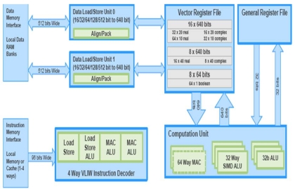
EETimes – Tensilica described a new integer DSP core for next-generation cellular applications that when made in a 28nm process can compute 100 GMACs/second at less than a Watt. The BBE64 core is a new instruction set architecture based on the companies’ current Xtensa LX4 core.
The BBE64 combines SIMD and VLIW concepts and lets designers configure processors for a range of handset and base stations uses. Rowen said the core run at data rates of “a few hundred MHz” could process 2×2 MIMO LTE Advanced signals at 1 Gbit/second across 100 MHz of spectrum.
Texas Instruments ships chips using an array of eight DSP cores that computes 320 GMACs/second and 160 GFlops. TI uses a single core that handles both integer and floating point math.
Using separate integer and floating point cores would cost extra die area and power, one TI engineer said. Integer math lacks the accuracy of floating point calculations and would require programmers to make complex conversions, he said.
Tensilica is playing catch up with DSP core designer Ceva in the burgeoning cellular sector. Ceva commands as much as 90 percent of the business for licensed DSP cores in cellphone baseband processors, according to Will Strauss, principal of Forward Concepts. Ceva became the largest cellular baseband provider last fall, surpassing Qualcomm and others.
If you liked this article, please give it a quick review on ycombinator or StumbleUpon. Thanks

Brian Wang is a Futurist Thought Leader and a popular Science blogger with 1 million readers per month. His blog Nextbigfuture.com is ranked #1 Science News Blog. It covers many disruptive technology and trends including Space, Robotics, Artificial Intelligence, Medicine, Anti-aging Biotechnology, and Nanotechnology.
Known for identifying cutting edge technologies, he is currently a Co-Founder of a startup and fundraiser for high potential early-stage companies. He is the Head of Research for Allocations for deep technology investments and an Angel Investor at Space Angels.
A frequent speaker at corporations, he has been a TEDx speaker, a Singularity University speaker and guest at numerous interviews for radio and podcasts. He is open to public speaking and advising engagements.