
Stanford researchers started with a tiny platter of silicon to provide a support (substrate) for their experimental transistor. They dipped the silicon platter into a solution of DNA derived from bacteria and used a known technique to comb the DNA strands into relatively straight lines.
Next, the DNA on the platter was exposed to a copper salt solution. The chemical properties of the solution allowed the copper ions to be absorbed into the DNA.
Next the platter was heated and bathed in methane gas, which contains carbon atoms. Once again chemical forces came into play to aid in the assembly process. The heat sparked a chemical reaction that freed some of the carbon atoms in the DNA and methane. These free carbon atoms quickly joined together to form stable honeycombs of graphene.
“The loose carbon atoms stayed close to where they broke free from the DNA strands, and so they formed ribbons that followed the structure of the DNA,” Yap said.
So part one of the invention involved using DNA to assemble ribbons of carbon. But the researchers also wanted to show that these carbon ribbons could perform electronic tasks. So they made transistors on the ribbons.
“We demonstrated for the first time that you can use DNA to grow narrow ribbons and then make working transistors,” Sokolov said.

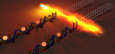
To the right is a honeycomb of graphene atoms. To the left is a double strand of DNA. The white spheres represent copper ions integral to the chemical assembly process. The fire represents the heat that is an essential ingredient in the technique. (Anatoliy Sokolov)
“This technique is very unique and takes advantage of the use of DNA as an effective template for controlled growth of electronic materials,” Javey said. “In this regard the project addresses an important research need for the field.”
Bao said the assembly process needs a lot of refinement. For instance, not all of the carbon atoms formed honeycombed ribbons a single atom thick. In some places they bunched up in irregular patterns, leading the researchers to label the material graphitic instead of graphene.
Even so, the process, about two years in the making, points toward a strategy for turning this carbon-based material from a curiosity into a serious contender to succeed silicon.
“Our DNA-based fabrication method is highly scalable, offers high resolution and low manufacturing cost,” said co-author Yap. “All these advantages make the method very attractive for industrial adoption.”
ABSTRACT
Graphene, laterally confined within narrow ribbons, exhibits a bandgap and is envisioned as a next-generation material for high-performance electronics. To take advantage of this phenomenon, there is a critical need to develop methodologies that result in graphene ribbons less than 10 nm in width. Here we report the use of metal salts infused within stretched DNA as catalysts to grow nanoscopic graphitic nanoribbons. The nanoribbons are termed graphitic as they have been determined to consist of regions of sp2 and sp3 character. The nanoscopic graphitic nanoribbons are micrometres in length, less than 10 nm in width, and take on the shape of the DNA template. The DNA strand is converted to a graphitic nanoribbon by utilizing chemical vapor deposition conditions. Depending on the growth conditions, metallic or semiconducting graphitic nanoribbons are formed. Improvements in the growth method have potential to lead to bottom-up synthesis of pristine single-layer graphene nanoribbons.
19 pages of supplemental information
If you liked this article, please give it a quick review on ycombinator or StumbleUpon. Thanks

Brian Wang is a Futurist Thought Leader and a popular Science blogger with 1 million readers per month. His blog Nextbigfuture.com is ranked #1 Science News Blog. It covers many disruptive technology and trends including Space, Robotics, Artificial Intelligence, Medicine, Anti-aging Biotechnology, and Nanotechnology.
Known for identifying cutting edge technologies, he is currently a Co-Founder of a startup and fundraiser for high potential early-stage companies. He is the Head of Research for Allocations for deep technology investments and an Angel Investor at Space Angels.
A frequent speaker at corporations, he has been a TEDx speaker, a Singularity University speaker and guest at numerous interviews for radio and podcasts. He is open to public speaking and advising engagements.